


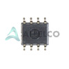
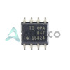

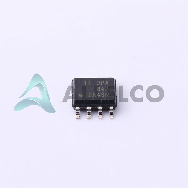
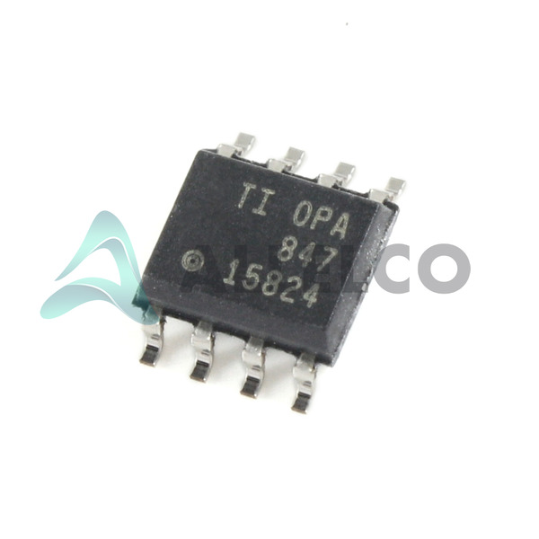
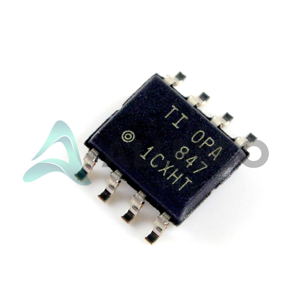
OPA847IDR (1)
Manufacturer Part Number
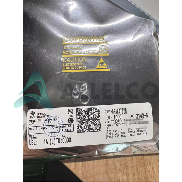
OPA847IDR
Manufacturer
Texas Instruments
OPA847IDR (2)
Introduction
The OPA847IDR is a high-performance, wideband operational amplifier (op-amp) designed for instrumentation, video, and high-speed applications.
Product Features and Performance
Gain Bandwidth Product: 3.9 GHz
Voltage Supply Span: 5 V to 12 V
Current Supply: 18.1 mA
Slew Rate: 950 V/s
Input Offset Voltage: 100 µV
Amplifier Type: Voltage Feedback
Output Current: 100 mA
Input Bias Current: 19 µA
OPA847IDR (3)
Product Advantages
Exceptional wideband performance
High slew rate and gain bandwidth
Low input offset voltage and bias current
Suitable for high-speed, high-precision applications
Key Technical Parameters
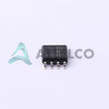
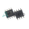
Package: 8-SOIC (0.154", 3.90mm Width)
Mounting Type: Surface Mount
Operating Temperature: -40°C to 85°C
OPA847IDR (4)
Quality and Safety Features
RoHS3 Compliant
Compatibility
Widely compatible with various electronic systems and circuits that require high-performance op-amps.
OPA847IDR (5)
Application Areas
Instrumentation
Video
High-speed applications
Product Lifecycle
The OPA847IDR is an active, in-production part. There are no plans for discontinuation, and replacement options are available if needed.
Several Key Reasons to Choose This Product
Excellent wideband performance with a large gain bandwidth product and high slew rate
Low input offset voltage and bias current for high-precision applications
Suitable for a wide range of operating voltages and temperatures
RoHS3 compliance for use in modern, environmentally-friendly electronics
Widely compatible with various electronic systems and circuits


 OPA855IDSGRTexas InstrumentsIC OPAMP GP 1 CIRCUIT 8WSON
 OPA857EVMTexas InstrumentsEVAL MODULE FOR OPA857
 OPA855DSGEVMTexas InstrumentsDEVELOPMENT AMPLIFIER
 OPA855QDSGRQ1Texas InstrumentsIC OPAMP GP 1 CIRCUIT 8WSON
 OPA856IDSGRTexas InstrumentsIC OPAMP GP 1 CIRCUIT 8WSON
 OPA847IDBVTG4Texas InstrumentsIC OPAMP VFB 1 CIRCUIT SOT23-6
 OPA855IDSGTTexas InstrumentsIC OPAMP GP 1 CIRCUIT 8WSON
 OPA857EVM-978Texas InstrumentsEVALUATION MODULE
 OPA857IRGTRTexas InstrumentsIC OPAMP GP 1 CIRCUIT 16VQFN


