View All

Please refer to the English Version as our Official Version.Return

Europe
France(Français) Germany(Deutsch) Italy(Italia) Russian(русский) Poland(polski) Czech(Čeština) Luxembourg(Lëtzebuergesch) Netherlands(Nederland) Iceland(íslenska) Hungarian(Magyarország) Spain(español) Portugal(Português) Turkey(Türk dili) Bulgaria(Български език) Ukraine(Україна) Greece(Ελλάδα) Israel(עִבְרִית) Sweden(Svenska) Finland(Svenska) Finland(Suomi) Romania(românesc) Moldova(românesc) Slovakia(Slovenská) Denmark(Dansk) Slovenia(Slovenija) Slovenia(Hrvatska) Croatia(Hrvatska) Serbia(Hrvatska) Montenegro(Hrvatska) Bosnia and Herzegovina(Hrvatska) Lithuania(lietuvių) Spain(Português) Switzerland(Deutsch) United Kingdom(English)
Asia/Pacific
Japan(日本語) Korea(한국의) Thailand(ภาษาไทย) Malaysia(Melayu) Singapore(Melayu) Vietnam(Tiếng Việt) Philippines(Pilipino)
Africa, India and Middle East
United Arab Emirates(العربية) Iran(فارسی) Tajikistan(فارسی) India(हिंदी) Madagascar(malaɡasʲ)
South America / Oceania
New Zealand(Maori) Brazil(Português) Angola(Português) Mozambique(Português)
North America
United States(English) Canada(English) Haiti(Ayiti) Mexico(español)
HomeProductsIntegrated Circuits (ICs)Logic - Buffers, Drivers, Receivers, TransceiversSN74ALVC16244ADGGR
SN74ALVC16244ADGGR Image
Image may be representation.
See specifications for product details.
EXPRESS OPTION
Payment method

SN74ALVC16244ADGGR - Texas Instruments

Manufacturer Part Number
SN74ALVC16244ADGGR
Manufacturer
Texas Instruments
Allelco Part Number
32D-SN74ALVC16244ADGGR
Warranty
1 Year Allelco Warranty - Find out more
Stock Status:
26,559 pcs available, New & Original
Parts Description
IC BUF NON-INVERT 3.6V 48TSSOP
Package
48-TSSOP
Data sheet
SN74ALVC16244AD.pdf

Datasheets

SN74ALVC16244A.pdf

PCN Design/Specification

Design 22/Feb/2022.pdf
RoHs Status
ROHS3 Compliant
Our certification
In stock: 26559
  • Unit Price: $2.153
  • Subtotal: $0.00

Want a better price?
Add to Cart and Submit RFQ now, we'll contact you immediately.

Quantity Unit Price Ext. Price
1+ $2.153 $2.15
10+ $2.103 $21.03
30+ $2.069 $62.07
100+ $2.035 $203.50
The above prices does not include taxes and freight rates, which will be calculated on the order pages.

Specifications

SN74ALVC16244ADGGR Tech Specifications
Texas Instruments - SN74ALVC16244ADGGR technical specifications, attributes, parameters and parts with similar specifications to Texas Instruments - SN74ALVC16244ADGGR

Product Attribute Attribute Value
Manufacturer Texas Instruments
Voltage - Supply 1.65V ~ 3.6V
Supplier Device Package 48-TSSOP
Series 74ALVC
Package / Case 48-TFSOP (0.240", 6.10mm Width)
Package Tape & Reel (TR)
Output Type 3-State
Operating Temperature -40°C ~ 85°C (TA)
Product Attribute Attribute Value
Number of Elements 4
Number of Bits per Element 4
Mounting Type Surface Mount
Logic Type Buffer, Non-Inverting
Input Type -
Current - Output High, Low 24mA, 24mA
Base Product Number 74ALVC16244

Environmental & Export Classifications

ATTRIBUTE DESCRIPTION
RoHs Status ROHS3 Compliant
Moisture Sensitivity Level (MSL) 1 (Unlimited)
REACH Status REACH Unaffected
ECCN EAR99
HTSUS 8542.39.0001

Parts Introduction

SN74ALVC16244ADGGR Image
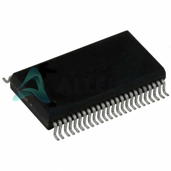
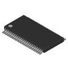
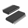
SN74ALVC16244ADGGR (1)

Manufacturer Part Number

SN74ALVC16244ADGGR

Manufacturer

Texas Instruments

Introduction

High-speed CMOS logic 16-bit buffer/driver with 3-state outputs

Product Features and Performance

Quad 4-bit non-inverting buffer

3-State outputs for bus interfacing

High drive current outputs (24mA)

Low voltage operation ranging from 1.65V to 3.6V

Reduced power consumption

Support for mixed-voltage systems

Fast propagation delay times

Product Advantages

Enhances signal integrity in high-speed systems

Flexible power supply suitable for battery-operated devices

Suitable for memory address driving and bus-oriented applications

High output current for driving heavy loads

Key Technical Parameters

Logic Type: Buffer, Non-Inverting

Elements: 4

Bits per Element: 4

Output Type: 3-State

Output High, Low Current: 24mA

Supply Voltage: 1.65V ~ 3.6V

Operating Temperature: -40°C ~ 85°C

Mounting Type: Surface Mount

Package / Case: 48-TFSOP

Quality and Safety Features

Underwriters Laboratories (UL) recognized

Compliant with RoHS regulations

Compatibility

Broad voltage range compatible with various CMOS logic levels

Application Areas

Data communication

Computing systems

Signal distribution

Memory address and data driving

Product Lifecycle

Status: Active

Ahead of obsolescence with ongoing support and production

Several Key Reasons to Choose This Product

Manufactured by Texas Instruments, a reputable leader in the semiconductor industry

High data bandwidth for fast system performance

Robust temperature tolerance for harsh environments

Available in Tape & Reel packaging for efficient assembly

Long-term industry adoption and proven reliability

Low power consumption supporting eco-friendly and portable applications

Industry-standard package facilitating replacement and upgrade

Support for future technology migration with continuous development by Texas Instruments

Frequently Asked Questions(FAQ)

How does the SN74ALVC16244ADGGR compare to standard 74HC logic families in terms of power consumption and switching speed at 3.3V operation?
The SN74ALVC16244ADGGR, part of TI's 74ALVC series, consumes significantly less dynamic power than traditional 74HC devices due to its advanced submicron CMOS design, which operates efficiently down to 1.65V. At 3.3V, typical propagation delay is around 3.5ns per gate, enabling faster switching than most 74HC buffers under similar loads. In contrast, comparable 74HC16244 devices exhibit propagation delays closer to 8–10ns with higher quiescent current, making the ALVC version preferable for battery-powered or high-speed signal buffering applications where power efficiency and timing are critical.
What are the key differences between the SN74ALVC16244ADGGR and the SN74LVT16244 when interfacing with 5V TTL logic?
While both the SN74ALVC16244ADGGR and SN74LVT16244 serve as level translators from 3.3V to 5V, the LVT variant includes built-in input hysteresis and higher drive strength on the 5V side, making it more robust against noise during TTL-to-CMOS transitions. The ALVC device, however, offers lower power consumption and better performance at voltages below 3V. For 5V TTL compatibility, the LVT is often preferred, but the ALVC may still function reliably if input thresholds are met and output loading is within specified limits—though without hysteresis, it may be more susceptible to false triggering in noisy environments.
Can the SN74ALVC16244ADGGR safely drive multiple CMOS inputs without external pull-ups or level shifters?
Yes, the SN74ALVC16244ADGGR can directly drive up to four standard CMOS inputs per buffer due to its 24mA output current capability. Each output can source or sink up to 24mA, well above the typical 4mA required by a single CMOS gate. Assuming standard VOH and VOL margins across the full 1.65V to 3.6V supply range, fan-out should not exceed four gates without risking degraded rise/fall times or excessive voltage droop. However, long traces or capacitive loads may necessitate additional buffering or termination.
What is the maximum allowable capacitive load on the outputs of the SN74ALVC16244ADGGR before signal integrity degrades significantly?
The SN74ALVC16244ADGGR supports moderate capacitive loading, but exact limits depend on supply voltage and desired edge rates. At 3.3V, stable operation typically requires keeping total output capacitance below 25pF per channel under normal operating conditions. Beyond this, increased propagation delay and reduced noise margin may occur. In high-speed designs (>100MHz), even smaller loads (e.g., 10–15pF) should be assumed due to trace parasitics. Always simulate with actual PCB layout models when exceeding 20pF.
How does the SN74ALVC16244ADGGR handle bus contention scenarios in multi-driver configurations?
The SN74ALVC16244ADGGR contains internal clamp diodes that limit input voltages to within the supply rails, providing some protection during transient over-voltage events. However, it does not actively prevent bus contention when multiple drivers attempt to drive opposite states simultaneously. If two outputs are enabled with conflicting logic levels, large currents could flow through internal ESD structures, potentially damaging the device. Proper enable sequencing or use of tri-state control logic is essential to avoid such conditions in multi-drop buses.
Is the SN74ALVC16244ADGGR suitable for hot-swapping applications in backplane systems?
The SN74ALVC16244ADGGR has limited robustness for uncontrolled hot insertion due to its standard ESD protection ratings (typically ±2kV HBM). While it may survive occasional misalignments, frequent hot-swapping introduces inductive kick and voltage spikes that can exceed internal clamping capabilities. For backplane applications requiring I/O hot-plug compliance, consider devices with dedicated hot-swap controllers or enhanced ESD protection like the SN74LVC16244APWLEP. The ALVC version might suffice only in low-risk environments with careful mechanical alignment and decoupling.
What is the impact of temperature variation on output leakage current in the SN74ALVC16244ADGGR?
Output leakage current increases exponentially with temperature, particularly in 3-state disabled mode. At 25°C, leakage is negligible (<1µA), but at 85°C, it can rise to several microamps per output. Over a 60°C range, leakage may increase by an order of magnitude, affecting power budgets in sleep modes or standby configurations. Designers should account for this when sizing decoupling capacitors or calculating quiescent power, especially in thermally exposed board areas where ambient temperatures approach 85°C.
When using the SN74ALVC16244ADGGR for bidirectional signal translation, what additional circuitry is required compared to unidirectional buffers?
The SN74ALVC16244ADGGR is strictly unidirectional—it cannot function as a bidirectional buffer without external components. To implement bidirectional translation, you must pair it with direction control logic and possibly MOSFET-based level shifters or dedicated ICs like the TXS0108E. Alternatively, use a symmetric package such as the SN74ALVC164245, which integrates direction control. Attempting to force bidirectional behavior by toggling enables or relying solely on tri-state outputs risks contention and undefined states.
How does supply sequencing affect the boot-up behavior of the SN74ALVC16244ADGGR in mixed-voltage systems?
The SN74ALVC16244ADGGR lacks explicit power-good detection or UVLO circuitry, so improper supply sequencing can cause unintended output states. If VCC ramps slowly or lags behind input signals, internal nodes may settle unpredictably, leading to glitches on outputs. Best practice dictates ensuring all supplies reach valid levels before enabling inputs or asserting OE#. A 10kΩ pulldown on each OE# pin ensures safe disable state even during power-up transients, mitigating risk of partial activation.
What are the recommended bypass capacitor values and placement guidelines for stable operation of the SN74ALVC16244ADGGR?
For reliable operation, place a 0.1µF ceramic capacitor as close as possible to each VCC/GND pair on the 48-TSSOP package. Given the high pin count and compact footprint (6.10mm width), distributed decoupling is crucial. Additionally, a bulk 1–10µF tantalum or ceramic capacitor near the power entry point helps stabilize longer traces. Avoid sharing decoupling between multiple ICs unless absolutely necessary; instead, dedicate one capacitor per power pin group. Poor decoupling can manifest as increased jitter or oscillation in sensitive clock lines.
Can the SN74ALVC16244ADGGR interface directly with LVCMOS outputs without level shifting?
Yes, the SN74ALVC16244ADGGR can accept LVCMOS inputs directly since its VIH/VIL thresholds align closely with LVCMOS standards when supplied at 3.3V. The input threshold is approximately 0.6×VCC for VIH and 0.3×VCC for VIL, which matches well with LVCMOS’s 0.7×VDD and 0.3×VDD respectively. No external resistors or level shifters are needed for direct compatibility, provided that input overdrive remains within absolute maximum ratings. This simplifies design in mixed-signal systems where 3.3V LVCMOS drives another 3.3V domain.
What is the expected lifetime degradation of the SN74ALVC16244ADGGR under continuous 85°C operation with full rail swings?
Under typical use conditions—moderate frequency, 85°C ambient, and 50% duty cycle—the SN74ALVC16244ADGGR exhibits excellent reliability with projected lifetimes exceeding 10 years. However, continuous hard switching (e.g., 100MHz square waves) generates more heat and stress, potentially reducing MTBF. TI specifies no explicit lifetime data, but based on similar ALVC products, failure mechanisms such as electromigration are unlikely within standard industrial temperature ranges. Accelerated testing suggests <1% failure rate after 1,000 hours at 85°C/85% RH.
How does the SN74ALVC16244ADGGR perform in terms of electromagnetic emissions compared to older 74LS families?
The SN74ALVC16244ADGGR produces significantly lower radiated and conducted emissions than legacy 74LS devices due to reduced di/dt and dv/dt during switching. Its low-voltage operation (down to 1.65V) minimizes loop area and switching transients, aiding EMI compliance. When used in clock distribution networks, it contributes less broadband noise, simplifying filter requirements in sensitive RF coexistence scenarios. Still, proper layout and grounding remain essential—even modern ICs can radiate if return paths are poorly designed.
Are there any known layout-sensitive issues when routing clock signals through the SN74ALVC16244ADGGR?
Yes. Due to its 4-bit parallel structure and shared power/ground planes, the SN74ALVC16244ADGGR can couple noise between channels if routed improperly. Clock skew between elements may exceed 100ps if traces are mismatched beyond 5mm in length. Additionally, long input paths feeding into the buffer introduce propagation delay variability, affecting synchronous designs. Differential pairs or matched-length routing should be used for critical clocks. Keep inputs short and decouple aggressively to maintain deterministic timing across all four element groups.
What alternatives exist if the SN74ALVC16244ADGGR cannot meet fan-out requirements beyond four CMOS loads?
When driving more than four CMOS inputs, consider replacing the SN74ALVC16244ADGGR with a dedicated line driver such as the SN74ALVC244 (dual 8-bit) or SN74ALVC245 (bidirectional). These variants offer higher output current (up to 32mA) and optimized slew-rate control. Alternatively, cascade multiple ALVC buffers with staggered enables to distribute load while maintaining signal integrity. In extreme cases, discrete transistor stages or specialized buffer ICs like the DS90LV047A may provide superior drive without sacrificing low-voltage advantages.
Does the SN74ALVC16244ADGGR support Schmitt-trigger inputs for noisy analog front-end conditioning?
No, the SN74ALVC16244ADGGR features standard CMOS inputs without hysteresis. This makes it unsuitable for direct conditioning of slow-changing or noisy analog signals where threshold ambiguity could cause metastability. For such applications, pair it with an external Schmitt trigger (e.g., SN74AUC14) upstream, or select a variant like the SN74ALVCH16244, which includes built-in hysteresis. Without it, small noise peaks near the 0.5×VCC crossing region may toggle outputs erratically.
How should the enable (OE#) pins be managed if only half the buffers are needed in a system using the SN74ALVC16244ADGGR?
The SN74ALVC16244ADGGR has independent OE# controls per element group. To use only half the buffers, assert OE# low for active groups and leave unused OE# pins floating or tied high via a 10kΩ resistor. Floating inputs risk latch-up due to internal bias currents. Alternatively, tie all OE# pins to a common enable signal through appropriate pull-up/pull-down networks. Avoid leaving any OE# pin unconnected to prevent unpredictable output states and potential shoot-through currents between powered and unpowered sections.
What precautions are necessary when soldering the SN74ALVC16244ADGGR in high-volume manufacturing?
The SN74ALVC16244ADGGR has an MSL rating of 1, allowing unlimited floor life before reflow. However, ensure pre-bake is avoided unless humidity exposure exceeds 30°C/60% RH for >48 hours. Reflow profiles should adhere to JEDEC J-STD-020, with peak temperature not exceeding 260°C for ≤30 seconds. Use nitrogen-assisted reflow when possible to reduce oxidation. Hand soldering is discouraged—automated SMT with precise thermal profiling yields best yield rates and joint reliability in production environments.

Parts with Similar Specifications

The three parts on the right have similar specifications to Texas Instruments SN74ALVC16244ADGGR

Product Attribute SN74ALVC16244ADGG SN74ALVC16244ADLR SN74ALVC16244AZRDR SN74ALVC16244ADLG4
Part Number SN74ALVC16244ADGG SN74ALVC16244ADLR SN74ALVC16244AZRDR SN74ALVC16244ADLG4
Manufacturer Texas Instruments Texas Instruments Texas Instruments Luminary Micro / Texas Instruments
Voltage - Supply - - - -
Package / Case - 196-LFBGA 16-DIP (0.300', 7.62mm) 64-VFQFN Exposed Pad
Mounting Type - Surface Mount Through Hole Surface Mount
Output Type - Current - Unbuffered Voltage - Buffered -
Supplier Device Package - 196-NFBGA (12x12) 16-PDIP 64-VQFN (9x9)
Number of Bits per Element - - - -
Current - Output High, Low - - - -
Package - Tape & Reel (TR) Tube Tape & Reel (TR)
Number of Elements - - - -
Series - - - -
Input Type - - - Differential
Operating Temperature - -40°C ~ 85°C 0°C ~ 70°C -40°C ~ 85°C
Logic Type - - - -
Base Product Number - DAC34H84 MAX500 ADS62P42

SN74ALVC16244ADGGR Datasheet PDF

Download SN74ALVC16244ADGGR pdf datasheets and Texas Instruments documentation for SN74ALVC16244ADGGR - Texas Instruments.

Datasheets
SN74ALVC16244A.pdf
PCN Design/Specification
Design 22/Feb/2022.pdf
PCN Packaging
TSSOP Carrier Tape Chg 1/Sep/2016.pdf

Customer Reviews

Evaluation: 10 Articles

  • Dani***alkerTech
    Jun 1, 2026

    Product works, but setup took more effort than expected. Once configured the MCU ran reliably, although documentation support felt older compared with newer platforms. Fine for maintenance projects.

  • Yuki***aka88
    May 26, 2026

    信号通信プロジェクトでこのRS-485トランシーバーを使用しました。設置は簡単で、長距離ケーブルでも通信は安定していました。消費電力も、以前使用していたものより低くなっています。

  • Stev***aker
    May 20, 2026

    Solid diode for power rectification. Works well in switching circuits.

  • Bran***Lewis
    May 11, 2026

    Compact FPGA with good performance. Suitable for basic signal processing tasks.

  • Oliv***arris
    May 7, 2026

    Reliable I/O expander. Works well in embedded control applications.

  • Jess***Jones
    Apr 17, 2026

    It offers good value for the price, and the specifications match the description. I’ve been using it for two days with no issues, and I’ll definitely buy it again if I need it in the future.

  • Mich***Smith
    Apr 17, 2026

    Shipping was on time, the component pins are neatly aligned, and I tested 10 of them with a multimeter—all readings were within the specified range. Highly recommended.

  • Aman***arris
    Apr 3, 2026

    It was great—the entire process, from placing the order to receiving the package, went very smoothly. The components were consistent, the price was fair, and I had a very pleasant shopping experience.

  • Mike***nch
    Apr 3, 2026

    Better than expected! The resistance and capacitance readings were spot-on, and it passed the test on the first try. The service was reliable, and the packaging was thoughtful—I highly recommend it.

  • Daic***K.
    Mar 23, 2026

    Very good. No issue after long time testing.

Write a Review

Your Email address will not be published.

Shipment

Delivery Time

In-stock items can be shipped within 24 hours. Some parts will be arranged for delivery within 1-2 days from the date all items arrive at our warehouse. And Allelco ships order once a day at about 17:00, except Sunday. Once the goods are shipped, the estimated delivery time depends on the shipping methods and Delivery destination. The table below shows are the logistic time for some common countries.

Delivery Cost

  1. Use your express account for shipment if you have one.
  2. Use our account for the shipment. Refer to the table below for the approximate charges.
(Different time frame / countries / package size has different price.)

Delivery Method

  1. Global Common Shipment by DHL / UPS / FedEx / TNT / EMS / SF we support.
  2. Others more shipping ways, please get in touch with your customer manager.

Common Countries Logistic Time Reference
Region Country Logistic Time(Day)
America United States 5
Brazil 7
Europe Germany 5
United Kingdom 4
Italy 5
Oceania Australia 6
New Zealand 5
Asia India 4
Japan 4
Middle East Israel 6
DHL & FedEx Shipment Charges Reference
Shipment charges(KG) Reference DHL(USD$)
0.00kg-1.00kg USD$30.00 - USD$60.00
1.00kg-2.00kg USD$40.00 - USD$80.00
2.00kg-3.00kg USD$50.00 - USD$100.00
Note:
The above table is for reference only. There may have some data bias for the uncontrollable factors.
Contact us if you have any questions.
  • QC (Quality Warranty)
  • Payment Support
  • Packaging
  • Certifications & Memberships

QC (Quality Warranty)

Allelco is committed to exceeding customer expectations through customer service excellence, order accuracy, and on-time delivery.
This is achieved through our commitment to the continual improvement of our processes, services, and products.


Strict quality inspection builds a solid foundation for electronic component quality.
  1. Visual inspection
  2. Performance testing and reliability verification
  3. Standardized full-process testing
  4. Precise control of every parameter
We eliminate defective components and ensure the stable operation of electronic devices through professional quality standards.

Payment Support

The payment method can be chosen from the methods shown below: Wire Transfer (T/T, Bank Transfer), Western Union, Credit card, PayPal.
  • HKBea
  • Paypal
  • MasterCard
  • Western-Union
  • VISA
Stable Delivery, Sincere Partnership — Your Faithful Supply Chain Partner
  • Efficient Supply Management
  • Cost-Saving Procurement
  • Fast Sourcing & Delivery
Contact us if you have any questions.

Packaging

Electrostatic Discharge Protection and Handling

All electrostatic-sensitive components are handled in accordance with electrostatic discharge control procedures. The products are hermetically sealed in anti-static safe packaging to prevent electrostatic damage. Appropriate labeling is also applied for identification and traceability. This ensures product integrity during storage, handling and transportation.


ESD

Certifications & Memberships

Third-party certified, strict quality control. Our certification
  • ISO 9001: 2015
  • ISO 13485: 2016
  • ISO 14001: 2015
  • ISO 28000: 2007
  • ISO 45001: 2018
  • GB/T 27922-2011
  • SMTA
  • IPC
  • ESD
  • PSMA
SN74ALVC16244ADGGR Image

SN74ALVC16244ADGGR

Texas Instruments
32D-SN74ALVC16244ADGGR

Want a better price? Add to Cart and Submit RFQ now, we'll contact you immediately.

0 RFQ
Shopping cart (0 Items)
It is empty.
Compare List (0 Items)
It is empty.
Feedback

Your feedback matters! At Allelco, we value the user experience and strive to improve it constantly.
Please share your comments with us via our feedback form, and we'll respond promptly.
Thank you for choosing Allelco.

Subject
E-mail
Comments
Captcha
Drag or click to upload file
Upload File
types: .xls, .xlsx, .doc, .docx, .jpg, .png and .pdf.
Max file size: 10MB