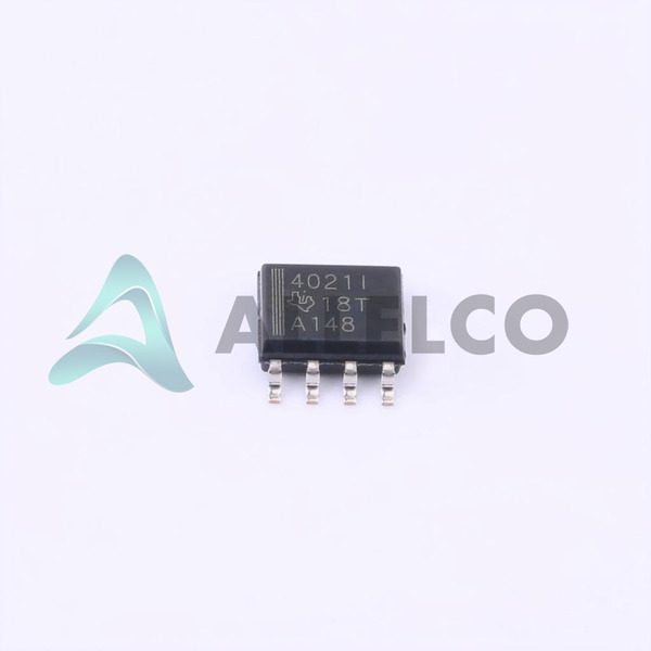
View All

Please refer to the English Version as our Official Version.Return

Europe
France(Français) Germany(Deutsch) Italy(Italia) Russian(русский) Poland(polski) Czech(Čeština) Luxembourg(Lëtzebuergesch) Netherlands(Nederland) Iceland(íslenska) Hungarian(Magyarország) Spain(español) Portugal(Português) Turkey(Türk dili) Bulgaria(Български език) Ukraine(Україна) Greece(Ελλάδα) Israel(עִבְרִית) Sweden(Svenska) Finland(Svenska) Finland(Suomi) Romania(românesc) Moldova(românesc) Slovakia(Slovenská) Denmark(Dansk) Slovenia(Slovenija) Slovenia(Hrvatska) Croatia(Hrvatska) Serbia(Hrvatska) Montenegro(Hrvatska) Bosnia and Herzegovina(Hrvatska) Lithuania(lietuvių) Spain(Português) Switzerland(Deutsch) United Kingdom(English)
Asia/Pacific
Japan(日本語) Korea(한국의) Thailand(ภาษาไทย) Malaysia(Melayu) Singapore(Melayu) Vietnam(Tiếng Việt) Philippines(Pilipino)
Africa, India and Middle East
United Arab Emirates(العربية) Iran(فارسی) Tajikistan(فارسی) India(हिंदी) Madagascar(malaɡasʲ)
South America / Oceania
New Zealand(Maori) Brazil(Português) Angola(Português) Mozambique(Português)
North America
United States(English) Canada(English) Haiti(Ayiti) Mexico(español)
HomeProductsIntegrated Circuits (ICs)Linear - Amplifiers - Instrumentation, OP Amps, Buffer AmpsTHS4021IDR
THS4021IDR Image
Image may be representation.
See specifications for product details.
EXPRESS OPTION
Payment method

THS4021IDR - Texas Instruments

Manufacturer Part Number
THS4021IDR
Manufacturer
Texas Instruments
Allelco Part Number
32D-THS4021IDR
Warranty
1 Year Allelco Warranty - Find out more
Stock Status:
7,789 pcs available, New & Original
Parts Description
IC VOLTAGE FEEDBACK 1 CIRC 8SOIC
Package
8-SOIC
Data sheet
THS4021IDR.pdf

PCN Design/Specification

THS402x Datasheet 23/May/2023.pdf

HTML Datasheet

THS4021/22.pdf
RoHs Status
ROHS3 Compliant
Our certification
In stock: 7789
  • Unit Price: $6.172
  • Subtotal: $0.00

Want a better price?
Add to Cart and Submit RFQ now, we'll contact you immediately.

Quantity Unit Price Ext. Price
1+ $6.172 $6.17
10+ $5.499 $54.99
30+ $5.068 $152.04
100+ $4.652 $465.20
The above prices does not include taxes and freight rates, which will be calculated on the order pages.

Specifications

THS4021IDR Tech Specifications
Texas Instruments - THS4021IDR technical specifications, attributes, parameters and parts with similar specifications to Texas Instruments - THS4021IDR

Product Attribute Attribute Value
Manufacturer Texas Instruments
Voltage - Supply Span (Min) 9 V
Voltage - Supply Span (Max) 32 V
Voltage - Input Offset 500 µV
Supplier Device Package 8-SOIC
Slew Rate 470V/µs
Series -
Package / Case 8-SOIC (0.154", 3.90mm Width)
Package Tape & Reel (TR)
Output Type -
Product Attribute Attribute Value
Operating Temperature -40°C ~ 85°C
Number of Circuits 1
Mounting Type Surface Mount
Current - Supply 7.8mA
Current - Output / Channel 100 mA
Current - Input Bias 3 µA
Base Product Number THS4021
Amplifier Type Voltage Feedback
-3db Bandwidth 350 MHz

Environmental & Export Classifications

ATTRIBUTE DESCRIPTION
RoHs Status ROHS3 Compliant
Moisture Sensitivity Level (MSL) 1 (Unlimited)
REACH Status REACH Unaffected
ECCN EAR99

Parts Introduction

THS4021IDR Image
THS4021IDR (1)

Manufacturer Part Number

THS4021IDR

Manufacturer

Texas Instruments

Introduction

High-speed, low-distortion, precision operational amplifier with rail-to-rail input/output, ideal for instrumentation and wideband applications.

Product Features and Performance

Extremely wide bandwidth of 350 MHz

Excellent slew rate of 470 V/µs

Low input offset voltage of 500 µV

Low input bias current of 3 µA

High output current drive of 100 mA

Wide supply voltage range of 9 V to 32 V

Stable operation with capacitive loads

Unity-gain stable

Product Advantages

Ideal for instrumentation, wideband, and high-speed applications

Delivers high performance with low distortion

Provides excellent precision and stability

Operates over a wide range of supply voltages

THS4021IDR Image
THS4021IDR (2)

Key Technical Parameters

Operating temperature range: -40°C to +85°C

Number of circuits: 1

Amplifier type: Voltage feedback

Supply current: 7.8 mA

Quality and Safety Features

RoHS3 compliant

Packaged in an 8-pin SOIC surface-mount package

Compatibility

Compatible with a wide range of applications and systems

Application Areas

Instrumentation and test equipment

Industrial control systems

High-speed data acquisition

Medical equipment

Audio and video processing

Product Lifecycle

This product is currently in production and available for purchase.

Replacement or upgrade options may be available in the future, but the manufacturer should be consulted for the latest information.

Key Reasons to Choose This Product

Exceptional bandwidth and slew rate for high-speed, high-performance applications

Excellent precision and stability with low input offset voltage and bias current

Wide supply voltage range and high output current drive capability

Stable operation with capacitive loads, making it suitable for a variety of applications

RoHS3 compliance for environmentally-friendly use
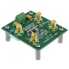
Frequently Asked Questions(FAQ)

How does the slew rate of the THS4021IDR compare to other high-speed voltage feedback amplifiers in its class, and what are the implications for driving large capacitive loads?
The THS4021IDR offers a slew rate of 470 V/µs, which places it among the higher-performing voltage feedback amplifiers suitable for fast transient response. When compared to amplifiers like the LT1228CN8#PBF (with similar bandwidth but lower slew rates), the THS4021IDR provides significantly faster edge transitions, making it advantageous in precision pulse or video applications where signal integrity over time is critical. However, this high slew rate can lead to increased overshoot and ringing when driving large capacitive loads due to reduced phase margin. Designers must consider compensation techniques or output buffering to mitigate instability, especially in closed-loop configurations above unity gain.
What is the typical input offset voltage of the THS4021IDR, and how might it affect precision analog signal conditioning at high frequencies?
The THS4021IDR has an input offset voltage of 500 µV, which is relatively low for a high-speed amplifier. In precision applications such as sensor signal conditioning or active filtering, this small offset translates into minimal DC error across the output. However, at frequencies approaching its 350 MHz bandwidth, even minor offsets can interact with noise and gain errors, potentially degrading effective resolution in systems requiring sub-millivolt accuracy. Careful layout and grounding are essential to prevent thermal drift and noise coupling from exacerbating offset effects during real-world operation.
Can the THS4021IDR be safely used in single-supply applications, and what supply voltage range should be considered for stable performance?
Yes, the THS4021IDR supports a supply voltage span from 9 V to 32 V, enabling use in both dual- and single-supply configurations. For single-supply designs, voltages between 12 V and 24 V are commonly employed to maintain headroom while ensuring rail-to-rail-like swing near the positive rail. Operating below 9 V may reduce available output range and degrade dynamic performance. It is important to verify that the input common-mode range and output swing specifications meet the required signal levels within the selected supply window to avoid clipping or distortion.
How does the current consumption of the THS4021IDR compare to alternative amplifiers like the AD8021ARZ-REEL, and what impact does this have on power-constrained designs?
The THS4021IDR draws approximately 7.8 mA of supply current, which is moderate compared to ultra-low-power alternatives but lower than some older high-speed op-amps. In contrast, the AD8021ARZ-REEL typically consumes around 6–8 mA under similar conditions, showing comparable efficiency. While both devices are efficient for their speed grade, the THS4021IDR’s slightly higher bias current relative to input offset may influence long-term drift in high-gain transimpedance stages. Designers must balance power budget against bandwidth and linearity needs in battery-powered or thermally sensitive systems.
What are the recommended layout practices when using the THS4021IDR in a PCB design, particularly regarding decoupling and thermal management?
Due to its surface-mount 8-SOIC package and high-speed characteristics, the THS4021IDR demands careful PCB layout. Decoupling capacitors of 0.1 µF and 10 µF should be placed as close as possible to the V+ and V− pins, with short traces to minimize inductance. Ground planes beneath the device help with heat dissipation and reduce electromagnetic interference. Thermal vias are beneficial if the application involves continuous full-load operation, though typical duty cycles rarely require extensive heatsinking given the modest power dissipation (~150 mW at ±15 V). Avoiding stubs and maintaining impedance-controlled paths is crucial to preserve bandwidth and stability.
Is the THS4021IDR suitable for driving heavy capacitive loads, and how might one determine the maximum allowable capacitance without oscillation?
The THS4021IDR can drive loads up to 100 mA per channel, but driving large capacitive loads without degradation requires caution. A rule of thumb is to ensure the loop gain remains sufficient to suppress peaking; typically, capacitances beyond 50 pF may necessitate series isolation resistors (e.g., 10–50 Ω) at the output. At unity gain, the device may become unstable with loads above 100 pF. Simulation tools such as TI's WEBENCH or SPICE models provide accurate phase margin predictions. Empirical testing with a network analyzer or oscilloscope is advised for final validation in production environments.
How does the bandwidth of the THS4021IDR compare to the LT1077IS8#PBF, and what trade-offs exist between speed and precision in these two amplifiers?
The THS4021IDR delivers a -3 dB bandwidth of 350 MHz, whereas the LT1077IS8#PBF offers significantly lower bandwidth (typically ~10 MHz), reflecting its design focus on precision rather than speed. This makes the THS4021IDR far superior in applications requiring high-frequency amplification, such as video processing or RF front ends. However, the LT1077 maintains better DC precision (lower input offset voltage and lower drift), making it preferable in instrumentation scenarios where accuracy dominates over bandwidth. Choosing between them depends on whether the system prioritizes dynamic response or static measurement fidelity.
What operating temperature range must be respected when deploying the THS4021IDR in industrial control systems, and how does this affect reliability?
The THS4021IDR is rated for industrial temperatures from -40°C to 85°C, ensuring reliable operation in harsh environments such as factory automation or outdoor sensing nodes. Within this range, key parameters like offset voltage and bias current remain stable, although slight increases in input offset can occur near the upper limit. Long-term reliability is enhanced by adherence to Moisture Sensitivity Level 1, allowing unlimited floor life before reflow. Thermal derating is generally not needed unless ambient temperatures exceed 70°C with poor airflow, which could accelerate electromigration in bond wires.
Can the THS4021IDR operate reliably in high-reliability aerospace applications, and what certifications support its deployment?
While the THS4021IDR itself is not radiation-hardened, it meets standard commercial aerospace requirements provided it is used within specified environmental limits. Its RoHS3 compliance, REACH unaffected status, and EAR99 classification simplify export and regulatory approval processes. For mission-critical aerospace designs, additional qualification testing (such as vibration, thermal cycling, and humidity exposure) would still be necessary. The device’s consistent performance across temperature and aging conditions supports its use in non-radiation-sensitive subsystems where size, weight, and power constraints favor high-performance linear solutions.
What substitutes are functionally compatible with the THS4021IDR, and how do they differ in terms of pin compatibility and performance characteristics?
Functional substitutes include the LT1228CN8#PBF, LT6018IS8E#PBF, LT1970ACFE#PBF, LT1077IS8#PBF, and AD8021ARZ-REEL. Among these, the LT1228 and AD8021 share similar bandwidth and slew rate profiles, making them viable drop-in replacements in many high-speed designs. However, differences in input offset (LT1077IS8#PBF: ~1 µV vs. THS4021IDR: 500 µV) and power consumption (LT6018: ultra-low quiescent current) create distinct trade-offs. Pin compatibility varies—some require different supply ranges or have reversed pinouts—so board redesign may be necessary. Always consult updated datasheets and perform functional verification before substituting.
How does the output current capability of the THS4021IDR compare to dedicated buffer stages like the LT1970ACFE#PBF, and what considerations apply when cascading stages?
The THS4021IDR provides up to 100 mA of output current per channel, which is robust for most general-purpose driving tasks. In contrast, the LT1970ACFE#PBF is optimized for ultra-low-noise, high-precision buffering and typically delivers lower output current (~20–30 mA). When cascading amplifier stages, impedance matching becomes critical: connecting a high-current driver like the THS4021IDR directly to a sensitive preamp stage can cause loading effects and signal loss. Inserting a series resistor or using matched impedances ensures signal transfer without compromising either stage’s intended performance.
What precautions should be taken when using the THS4021IDR in unity-gain configuration, and why is feedback stability particularly sensitive in this mode?
Unity-gain buffers are highly susceptible to oscillations due to reduced phase margin, especially with capacitive loads. The THS4021IDR, despite its high bandwidth, must be compensated externally if stability is compromised. Adding a small series resistor (e.g., 2–10 Ω) at the output helps dampen peaking. Additionally, minimizing parasitic capacitance on the output node and avoiding long PCB traces are essential. TI recommends evaluating loop gain with simulation or test equipment when operating near unity gain, as real-world parasitics often degrade theoretical performance.
How does the input bias current of the THS4021IDR compare to bipolar-input amplifiers, and what impact does this have on high-impedance sensor interfaces?
The THS4021IDR has an input bias current of 3 µA, which is typical for JFET-input FET op-amps. While much lower than bipolar junction transistor (BJT)-based designs, it is still significant in high-impedance circuits such as photodiode transimpedance amplifiers. For example, in a 1 MΩ feedback path, 3 µA creates a 3 V drop, completely saturating the output. In such cases, the LT1077IS8#PBF or other ultra-low-bias devices are preferred. The THS4021IDR is better suited to buffered sensor signals or low-Z sources where bias current errors are manageable.
What is the significance of the Moisture Sensitivity Level (MSL) 1 rating for the THS4021IDR, and how does this affect manufacturing handling procedures?
MSL 1 indicates that the THS4021IDR is not moisture-sensitive and can be stored indefinitely at room conditions without special drying prior to reflow soldering. This simplifies inventory management and reduces costs associated with baking components before assembly. It also allows manufacturers to use standard pick-and-place and reflow profiles without risk of delamination or popcorning. However, users should still follow IPC standards for handling all ICs, including proper ESD protection during manual assembly.
How does the package type (8-SOIC) of the THS4021IDR influence thermal performance compared to larger packages like SOIC-16 or TSSOP?
The 8-SOIC package provides adequate thermal dissipation for the THS4021IDR under typical operating conditions, with a thermal resistance (θJA) around 120°C/W. Larger packages like SOIC-16 offer lower θJA due to increased copper area, improving heat spreading. However, the 8-pin form factor saves board space and aligns with compact design trends. For most applications drawing less than 100 mW, passive cooling suffices. If higher power dissipation is expected, adding a ground plane or thermal pad improves junction-to-ambient performance without changing package type.
Can the THS4021IDR be used in differential amplifier configurations, and what limitations arise from its internal architecture?
Yes, the THS4021IDR can be configured as a differential amplifier using standard resistor networks. However, its voltage-feedback topology means that matching precision of external resistors directly impacts CMRR. At 350 MHz, even 0.1% tolerance resistors can introduce noticeable mismatch, degrading rejection of common-mode noise. Additionally, the limited output swing near rails (especially at high speeds) constrains dynamic range. For best results, use laser-trimmed resistors and symmetric layout. Performance will generally trail that of fully differential amplifiers like the OPA197 or ADA4940 in high-fidelity ADC driver applications.
What role does the base product number THS4021 play in selecting compatible evaluation boards or reference designs?
The base product number THS4021 identifies the family of devices sharing core architecture, including variants like the THS4021IDR. Texas Instruments provides evaluation modules (e.g., EVMs) based on this base number, enabling rapid prototyping. These boards include optimized layouts, decoupling networks, and test points tailored to the amplifier’s bandwidth and slew characteristics. Using an EVM accelerates design validation and ensures adherence to recommended practices, reducing risk of instability or EMI issues in early development phases.
How does the THS4021IDR perform in terms of harmonic distortion compared to other wideband amplifiers like the LT6018IS8E#PBF, and what factors influence linearity at high frequencies?
The THS4021IDR exhibits moderate harmonic distortion (THD ~ -60 dBc at 10 MHz), suitable for many communication and imaging applications. In comparison, the LT6018IS8E#PBF trades bandwidth for lower distortion but operates at much lower frequencies (~1 MHz). At high frequencies, nonlinearities arise from internal transistor saturation and slew-induced compression. Even with ideal supplies, second-order effects like intermodulation increase with amplitude and frequency. To improve linearity, operate within specified output swing limits, avoid overdriving inputs, and consider predistortion or feedback calibration in precision systems.

Parts with Similar Specifications

The three parts on the right have similar specifications to Texas Instruments THS4021IDR

Product Attribute THS4021ID THS4021CDR THS4021CDGNR THS4021IDG4
Part Number THS4021ID THS4021CDR THS4021CDGNR THS4021IDG4
Manufacturer Texas Instruments Texas Instruments Texas Instruments Luminary Micro / Texas Instruments
Amplifier Type - - - -
Mounting Type - Surface Mount Through Hole Surface Mount
Current - Output / Channel - - - -
Current - Input Bias - - - -
Package - Tape & Reel (TR) Tube Tape & Reel (TR)
Output Type - Current - Unbuffered Voltage - Buffered -
-3db Bandwidth - - - -
Operating Temperature - -40°C ~ 85°C 0°C ~ 70°C -40°C ~ 85°C
Voltage - Supply Span (Min) - - - -
Package / Case - 196-LFBGA 16-DIP (0.300', 7.62mm) 64-VFQFN Exposed Pad
Number of Circuits - - - -
Base Product Number - DAC34H84 MAX500 ADS62P42
Current - Supply - - - -
Voltage - Input Offset - - - -
Voltage - Supply Span (Max) - - - -
Supplier Device Package - 196-NFBGA (12x12) 16-PDIP 64-VQFN (9x9)
Series - - - -
Slew Rate - - - -

THS4021IDR Datasheet PDF

Download THS4021IDR pdf datasheets and Texas Instruments documentation for THS4021IDR - Texas Instruments.

PCN Design/Specification
THS402x Datasheet 23/May/2023.pdf
HTML Datasheet
THS4021/22.pdf

Customer Reviews

Evaluation: 10 Articles

  • Dani***alkerTech
    Jun 1, 2026

    Product works, but setup took more effort than expected. Once configured the MCU ran reliably, although documentation support felt older compared with newer platforms. Fine for maintenance projects.

  • Yuki***aka88
    May 26, 2026

    信号通信プロジェクトでこのRS-485トランシーバーを使用しました。設置は簡単で、長距離ケーブルでも通信は安定していました。消費電力も、以前使用していたものより低くなっています。

  • Stev***aker
    May 20, 2026

    Solid diode for power rectification. Works well in switching circuits.

  • Bran***Lewis
    May 11, 2026

    Compact FPGA with good performance. Suitable for basic signal processing tasks.

  • Oliv***arris
    May 7, 2026

    Reliable I/O expander. Works well in embedded control applications.

  • Jess***Jones
    Apr 17, 2026

    It offers good value for the price, and the specifications match the description. I’ve been using it for two days with no issues, and I’ll definitely buy it again if I need it in the future.

  • Mich***Smith
    Apr 17, 2026

    Shipping was on time, the component pins are neatly aligned, and I tested 10 of them with a multimeter—all readings were within the specified range. Highly recommended.

  • Aman***arris
    Apr 3, 2026

    It was great—the entire process, from placing the order to receiving the package, went very smoothly. The components were consistent, the price was fair, and I had a very pleasant shopping experience.

  • Mike***nch
    Apr 3, 2026

    Better than expected! The resistance and capacitance readings were spot-on, and it passed the test on the first try. The service was reliable, and the packaging was thoughtful—I highly recommend it.

  • Daic***K.
    Mar 23, 2026

    Very good. No issue after long time testing.

Write a Review

Your Email address will not be published.

Shipment

Delivery Time

In-stock items can be shipped within 24 hours. Some parts will be arranged for delivery within 1-2 days from the date all items arrive at our warehouse. And Allelco ships order once a day at about 17:00, except Sunday. Once the goods are shipped, the estimated delivery time depends on the shipping methods and Delivery destination. The table below shows are the logistic time for some common countries.

Delivery Cost

  1. Use your express account for shipment if you have one.
  2. Use our account for the shipment. Refer to the table below for the approximate charges.
(Different time frame / countries / package size has different price.)

Delivery Method

  1. Global Common Shipment by DHL / UPS / FedEx / TNT / EMS / SF we support.
  2. Others more shipping ways, please get in touch with your customer manager.

Common Countries Logistic Time Reference
Region Country Logistic Time(Day)
America United States 5
Brazil 7
Europe Germany 5
United Kingdom 4
Italy 5
Oceania Australia 6
New Zealand 5
Asia India 4
Japan 4
Middle East Israel 6
DHL & FedEx Shipment Charges Reference
Shipment charges(KG) Reference DHL(USD$)
0.00kg-1.00kg USD$30.00 - USD$60.00
1.00kg-2.00kg USD$40.00 - USD$80.00
2.00kg-3.00kg USD$50.00 - USD$100.00
Note:
The above table is for reference only. There may have some data bias for the uncontrollable factors.
Contact us if you have any questions.
  • QC (Quality Warranty)
  • Payment Support
  • Packaging
  • Certifications & Memberships

QC (Quality Warranty)

Allelco is committed to exceeding customer expectations through customer service excellence, order accuracy, and on-time delivery.
This is achieved through our commitment to the continual improvement of our processes, services, and products.


Strict quality inspection builds a solid foundation for electronic component quality.
  1. Visual inspection
  2. Performance testing and reliability verification
  3. Standardized full-process testing
  4. Precise control of every parameter
We eliminate defective components and ensure the stable operation of electronic devices through professional quality standards.

Payment Support

The payment method can be chosen from the methods shown below: Wire Transfer (T/T, Bank Transfer), Western Union, Credit card, PayPal.
  • HKBea
  • Paypal
  • MasterCard
  • Western-Union
  • VISA
Stable Delivery, Sincere Partnership — Your Faithful Supply Chain Partner
  • Efficient Supply Management
  • Cost-Saving Procurement
  • Fast Sourcing & Delivery
Contact us if you have any questions.

Packaging

Electrostatic Discharge Protection and Handling

All electrostatic-sensitive components are handled in accordance with electrostatic discharge control procedures. The products are hermetically sealed in anti-static safe packaging to prevent electrostatic damage. Appropriate labeling is also applied for identification and traceability. This ensures product integrity during storage, handling and transportation.


ESD

Certifications & Memberships

Third-party certified, strict quality control. Our certification
  • ISO 9001: 2015
  • ISO 13485: 2016
  • ISO 14001: 2015
  • ISO 28000: 2007
  • ISO 45001: 2018
  • GB/T 27922-2011
  • SMTA
  • IPC
  • ESD
  • PSMA
THS4021IDR Image

THS4021IDR

Texas Instruments
32D-THS4021IDR

Want a better price? Add to Cart and Submit RFQ now, we'll contact you immediately.

0 RFQ
Shopping cart (0 Items)
It is empty.
Compare List (0 Items)
It is empty.
Feedback

Your feedback matters! At Allelco, we value the user experience and strive to improve it constantly.
Please share your comments with us via our feedback form, and we'll respond promptly.
Thank you for choosing Allelco.

Subject
E-mail
Comments
Captcha
Drag or click to upload file
Upload File
types: .xls, .xlsx, .doc, .docx, .jpg, .png and .pdf.
Max file size: 10MB