
Manufacturer Part Number
THS4524MDBTREP
Manufacturer
Texas Instruments
Introduction
High-performance, low-power, rail-to-rail, precision operational amplifier
Ideal for a variety of industrial, medical, and instrumentation applications
Product Features and Performance
95 MHz gain-bandwidth product
145 MHz -3dB bandwidth
490 V/μs slew rate
5 mV input offset voltage
20 μA input bias current
55 mA output current per channel
Operates from 2.5 V to 5.5 V supplies
15 mA per channel supply current
Product Advantages
Excellent dynamic performance
High speed and precision
Low power consumption
Rail-to-rail input and output
Versatile applications
Key Technical Parameters
4 independent operational amplifiers in a single package
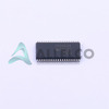
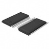
38-pin TSSOP package
Supports surface mount assembly
Operating temperature range: -55°C to 125°C
Quality and Safety Features
RoHS3 compliant
AEC-Q100 qualified for automotive applications
Compatibility
Suitable for a wide range of industrial, medical, and instrumentation applications
Application Areas
Precision measurement and control circuits
High-speed data acquisition systems
Medical instrumentation
Industrial process control
Communication systems
Product Lifecycle
Currently in active production
Replacement or upgrade options available from Texas Instruments
Key Reasons to Choose This Product
Exceptional speed, precision, and dynamic performance
Low power consumption for energy-efficient designs
Versatile 4-channel configuration for efficient board layout
Qualified for demanding industrial and automotive applications
Reliable and long-lasting solution from a trusted manufacturer


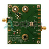 THS4531DGKEVMTexas InstrumentsEVAL MODULE FOR THS4531
 THS4531AIDGKTexas InstrumentsIC OPAMP DIFF 1 CIRCUIT 8VSSOP
 THS4531AIRUNRTexas InstrumentsIC OPAMP DIFF 1 CIRCUIT 10WQFN
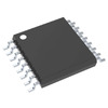 THS4522IPWTexas InstrumentsIC OPAMP DIFF 2 CIRCUIT 16TSSOP
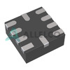 THS4531AIRUNTTexas InstrumentsIC OPAMP DIFF 1 CIRCUIT 10WQFN
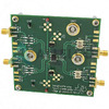 THS4522EVMTexas InstrumentsEVAL MODULE FOR THS4522
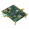 THS4531ADGKEVMTexas InstrumentsMODULE EVAL FOR THS4531A
 THS4531AIDGKRTexas InstrumentsIC OPAMP DIFF 1 CIRCUIT 8VSSOP
 THS4531AIDTexas InstrumentsIC OPAMP DIFF 1 CIRCUIT 8SOIC
 THS4522IPWRTexas InstrumentsIC OPAMP DIFF 2 CIRCUIT 16TSSOP
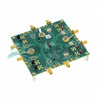 THS4524EVMTexas InstrumentsEVAL MODULE FOR THS4524
 THS4524IDBTRG4TI/BB


