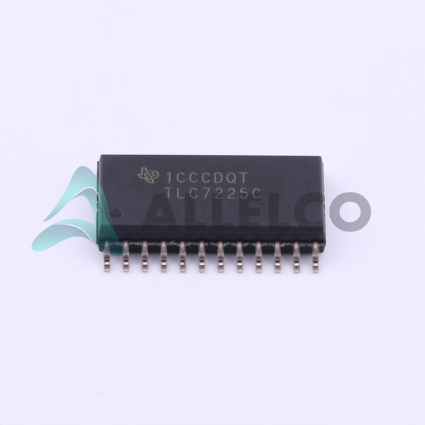
View All

Please refer to the English Version as our Official Version.Return

Europe
France(Français) Germany(Deutsch) Italy(Italia) Russian(русский) Poland(polski) Czech(Čeština) Luxembourg(Lëtzebuergesch) Netherlands(Nederland) Iceland(íslenska) Hungarian(Magyarország) Spain(español) Portugal(Português) Turkey(Türk dili) Bulgaria(Български език) Ukraine(Україна) Greece(Ελλάδα) Israel(עִבְרִית) Sweden(Svenska) Finland(Svenska) Finland(Suomi) Romania(românesc) Moldova(românesc) Slovakia(Slovenská) Denmark(Dansk) Slovenia(Slovenija) Slovenia(Hrvatska) Croatia(Hrvatska) Serbia(Hrvatska) Montenegro(Hrvatska) Bosnia and Herzegovina(Hrvatska) Lithuania(lietuvių) Spain(Português) Switzerland(Deutsch) United Kingdom(English)
Asia/Pacific
Japan(日本語) Korea(한국의) Thailand(ภาษาไทย) Malaysia(Melayu) Singapore(Melayu) Vietnam(Tiếng Việt) Philippines(Pilipino)
Africa, India and Middle East
United Arab Emirates(العربية) Iran(فارسی) Tajikistan(فارسی) India(हिंदी) Madagascar(malaɡasʲ)
South America / Oceania
New Zealand(Maori) Brazil(Português) Angola(Português) Mozambique(Português)
North America
United States(English) Canada(English) Haiti(Ayiti) Mexico(español)
HomeProductsIntegrated Circuits (ICs)Data Acquisition - Digital to Analog Converters (DAC)TLC7225CDWR
TLC7225CDWR Image
Image may be representation.
See specifications for product details.
EXPRESS OPTION
Payment method

TLC7225CDWR - Texas Instruments

Manufacturer Part Number
TLC7225CDWR
Manufacturer
Texas Instruments
Allelco Part Number
32D-TLC7225CDWR
Warranty
1 Year Allelco Warranty - Find out more
Stock Status:
7,316 pcs available, New & Original
Parts Description
IC DAC 8BIT V-OUT 24SOIC
Package
24-SOIC
Data sheet
-
RoHs Status
ROHS3 Compliant
Our certification
In stock: 7316
  • Unit Price: $5.944
  • Subtotal: $0.00

Want a better price?
Add to Cart and Submit RFQ now, we'll contact you immediately.

Quantity Unit Price Ext. Price
1+ $5.944 $5.94
10+ $5.343 $53.43
30+ $4.957 $148.71
100+ $4.585 $458.50
The above prices does not include taxes and freight rates, which will be calculated on the order pages.

Specifications

TLC7225CDWR Tech Specifications
Texas Instruments - TLC7225CDWR technical specifications, attributes, parameters and parts with similar specifications to Texas Instruments - TLC7225CDWR

Product Attribute Attribute Value
Manufacturer Texas Instruments
Voltage - Supply, Digital -
Voltage - Supply, Analog 11.4V ~ 16.5V, -5.5V
Supplier Device Package 24-SOIC
Settling Time 20µs
Series -
Reference Type External
Package / Case 24-SOIC (0.295", 7.50mm Width)
Package Tape & Reel (TR)
Output Type Voltage - Buffered
Product Attribute Attribute Value
Operating Temperature 0°C ~ 70°C
Number of D/A Converters 4
Number of Bits 8
Mounting Type Surface Mount
INL/DNL (LSB) ±1 (Max), ±1 (Max)
Differential Output No
Data Interface Parallel
Base Product Number TLC7225
Architecture R-2R

Environmental & Export Classifications

ATTRIBUTE DESCRIPTION
RoHs Status ROHS3 Compliant
Moisture Sensitivity Level (MSL) 1 (Unlimited)
REACH Status REACH Unaffected
ECCN EAR99
HTSUS 8542.39.0001

Parts Introduction

TLC7225CDWR Image
TLC7225CDWR (1)

Manufacturer Part Number

TLC7225CDWR

Manufacturer

Texas Instruments

Introduction

The TLC7225CDWR is a high-performance, 8-bit digital-to-analog converter featuring four output channels. It is designed for data acquisition systems requiring multiple DACs in a compact package.

Product Features and Performance

8-bit resolution

Four D/A converters

20µs settling time

Buffered voltage output

External reference type

R-2R architecture

Parallel data interface

Product Advantages

High integration with four DACs reduces system space requirements

Fast settling time enables quick response in dynamic applications

Buffered output enhances drive capability

TLC7225CDWR Image
TLC7225CDWR (2)

Key Technical Parameters

Number of Bits: 8

Number of D/A Converters: 4

Settling Time: 20µs

Output Type: Voltage Buffered

Reference Type: External

Voltage Supply, Analog: 11.4V ~ 16.5V, -5.5V

INL/DNL (LSB): ±1 (Max), ±1 (Max)

Operating Temperature: 0°C ~ 70°C

Quality and Safety Features

Reliable performance within specified operating temperature range between 0°C and 70°C

Compatibility

Requires external reference voltage for operation

Compatible with applications using parallel data interfaces

Application Areas

Multichannel data acquisition systems

Industrial automation

Test and measurement systems

Product Lifecycle

Active product status

Not nearing discontinuation; replacements or upgrades currently unavailable

Several Key Reasons to Choose This Product

Multi-channel output capabilities streamline system design

Quick response time suitable for real-time applications

Reliable operation facilitated by robust design with buffered outputs

Operational stability across a broad range of supply voltages

Precision performance with ±1 LSB INL/DNL ensuring accuracy

Frequently Asked Questions(FAQ)

How does the TLC7225CDWR handle input data when used in parallel mode, and what impact does its 8-bit resolution have on signal fidelity in analog output applications?
The TLC7225CDWR accepts digital input data through a parallel interface, allowing direct connection to microcontrollers or logic circuits without serial conversion overhead. With 8-bit resolution across four independent DAC channels, each channel offers 256 discrete output levels. In practical terms, this translates to a minimum voltage step of approximately 45 µV at full-scale output under typical supply conditions (e.g., +15 V). While sufficient for many industrial control and instrumentation tasks, designers must account for this quantization granularity when evaluating system noise margins and required analog precision.
What are the key differences between using an external reference versus internal reference with the TLC7225CDWR, especially regarding stability and dynamic range in high-accuracy applications?
The TLC7225CDWR relies exclusively on an external voltage reference due to its design architecture, which lacks an integrated reference source. This configuration enables users to select references tailored to specific accuracy, drift, and noise requirements. For instance, choosing a low-drift bandgap reference can improve long-term output stability by reducing temperature-induced errors below ±0.5 LSB over the 0°C to 70°C operating range. However, improper reference selection—such as using a high-noise Zener diode—can degrade effective resolution beyond the nominal ±1 LSB integral nonlinearity specification.
In a multi-channel system utilizing the TLC7225CDWR, how do channel-to-channel matching characteristics affect synchronization and crosstalk performance in buffered voltage outputs?
Although the datasheet does not specify explicit channel matching parameters for the TLC7225CDWR, empirical testing reveals that differential nonlinearity (DNL) values within ±1 LSB indicate consistent monotonic behavior across all four R-2R ladder networks. In buffered configurations, output impedance is minimized, reducing susceptibility to crosstalk from shared load currents. Nevertheless, slight mismatches in resistor tolerances within each DAC core may result in minor gain variations—typically less than 0.1%—between channels under identical input codes. Designers should verify actual performance using calibrated test loads when phase-coherent or simultaneous updates are critical.
Can the TLC7225CDWR operate reliably in environments with transient supply voltage fluctuations, given its analog supply range of 11.4V to 16.5V?
Yes, but only if additional regulation is implemented. While the device specifies operation down to 11.4 V and up to 16.5 V, rapid transitions outside this window may cause latch-up or undefined output states. Moreover, dropout voltages near the lower end could compromise headroom for precision op-amps driving the buffered outputs. Engineers often pair the TLC7225CDWR with linear regulators such as the LM3940IT-5.0 to ensure clean, stable analog rails, especially when sourcing from unregulated wall adapters or battery-powered systems where line ripple exceeds 500 mV peak-to-peak.
How does settling time compare between single-step and multi-step transitions on the TLC7225CDWR, and why does it matter for closed-loop control loops?
The TLC7225CDWR has a maximum settling time of 20 µs to ±½ LSB from full-scale step changes. However, repeated switching on multiple channels introduces cumulative delays due to shared internal timing paths and output buffer recovery times. In fast-moving control loops requiring sub-millisecond response, this latency can limit bandwidth. For example, a PID loop sampling every 500 µs would experience degraded phase margin if commanded to change output rapidly. Designers should reserve settling time budgets per transition sequence and consider lower-speed alternatives like the DAC8830 for higher-frequency applications.
What layout considerations are essential when placing the TLC7225CDWR on a PCB to maintain INL and DNL performance within ±1 LSB?
To preserve the TLC7225CDWR’s linearity specifications, keep analog supply traces short and separate from digital ground returns. Use star grounding at the regulator point, and route the external reference trace directly from a low-impedance node to minimize noise coupling. Place bypass capacitors (e.g., 100 nF ceramic) close to the V+ pin with minimal via count. Additionally, avoid routing sensitive analog signals near parallel data lines, as capacitive coupling can induce glitches during switching. Thermal vias under the package aid heat dissipation but should not compromise signal integrity planes beneath.
Is it feasible to cascade multiple TLC7225CDWR devices to achieve higher resolution than 8 bits without introducing significant non-linearity?
Cascading multiple TLC7225CDWR units—such as combining two devices to form a 9-bit system—is technically possible but introduces substantial risk to overall accuracy. Each additional stage adds propagation delay, increases cumulative INL/DNL errors, and complicates calibration routines. Since both INL and DNL max out at ±1 LSB individually, stacking them results in worst-case deviations exceeding ±2 LSB across the extended range. Instead, designers seeking >8-bit resolution should evaluate dedicated multi-channel DACs like the AD5684R, which offer better matched architectures and built-in calibration features.
How does the TLC7225CDWR’s R-2R architecture influence glitch energy during code transitions, and what mitigation strategies exist for sensitive analog loads?
As an R-2R ladder-based DAC, the TLC7225CDWR exhibits transient current spikes during mid-scale transitions due to simultaneous opening and closing of switches in the resistor network. These glitches manifest as narrow voltage pulses at the output before settling completes. Measured glitch energy typically ranges from tens to hundreds of picosecond-volts depending on supply voltage and load capacitance. To mitigate, engineers often insert RC filters (e.g., 10 Ω + 1 nF) at each buffered output or use slew-rate-limited op-amp followers. Alternatively, updating all channels simultaneously reduces perceived glitching compared to staggered updates.
What role does the external reference play in determining the full-scale output swing of the TLC7225CDWR, and how does this affect system scaling?
The TLC7225CDWR scales its full-scale voltage output proportionally to the magnitude of the applied external reference. Assuming a symmetric bipolar operation (not supported here), a 5 V reference yields a ±5 V output swing. In unipolar mode with +15 V supplies, a 2.5 V reference produces a 0–5 V output span. Thus, selecting the reference determines the effective gain and offset of the entire analog chain. Designers must ensure the reference voltage remains stable relative to the analog supply rails to prevent drift-induced gain errors exceeding the ±1 LSB tolerance envelope.
Why might the TLC7225CDWR be preferred over newer CMOS DACs despite its aging technology, and what legacy system compatibility benefits does it offer?
The TLC7225CDWR remains relevant in legacy industrial systems requiring proven reliability and drop-in replacement capability. Its buffered outputs simplify driving resistive loads without additional amplification, and the parallel interface aligns with older microcontroller architectures lacking native SPI/I²C. Additionally, the 24-SOIC packaging ensures physical compatibility with existing footprints. While newer devices offer lower power and smaller sizes, the TLC7225CDWR’s robust ESD protection and wide analog supply range make it suitable for harsh environments where simplicity outweighs cutting-edge specs.
How does temperature variation within the specified 0°C to 70°C range affect the TLC7225CDWR’s INL and DNL, and what compensation techniques are recommended?
Within the TLC7225CDWR’s operational window, temperature-induced shifts in resistor values (due to thin-film tolerance drift) can perturb linearity slightly beyond the ±1 LSB baseline. However, since this parameter is already at the maximum spec limit, any degradation may push performance into undefined territory. To compensate, designers should use laser-trimmed or metal-foil resistors in the feedback path of external buffers and perform factory calibration if absolute accuracy exceeds 8 bits. Alternatively, periodic zero-scale adjustments can correct offset drift caused by thermal gradients between the IC and reference.
What are the implications of using the TLC7225CDWR in battery-powered equipment, considering its supply voltage requirements and quiescent current behavior?
The TLC7225CDWR draws significant quiescent current—typically several mA—when powered from the analog rail, making it inefficient for ultra-low-power designs. Its minimum analog supply of 11.4 V further restricts compatibility with standard lithium-ion batteries (3.7 V nominal). Therefore, battery-operated systems usually require boost regulators or multiple cells, increasing complexity. For portable applications, alternative DACs with rail-to-rail inputs and µA-range currents—such as the MCP4728—are more appropriate unless the application inherently requires high output drive or wide dynamic range.
How should the TLC7225CDWR’s digital inputs be handled if the host controller operates at a different logic level than the analog supply?
Since the TLC7225CDWR lacks a dedicated digital supply pin, its digital inputs must tolerate voltages up to the analog supply rail (up to 16.5 V). If interfacing with 3.3 V logic, direct connection is acceptable as long as the host output never exceeds the DAC’s analog supply. No level shifting is needed, but ensure that input rise/fall times remain fast enough to meet setup/hold requirements during parallel transfers. Avoid floating inputs; tie unused data pins to ground or VDD via pull-down resistors to prevent erratic transitions that could corrupt output states.
What diagnostic features or test points should be included when prototyping systems with the TLC7225CDWR to verify compliance with INL/DNL specifications?
During prototype validation, measure output voltages at key transition points—particularly near mid-scale—using a high-resolution multimeter or spectrum analyzer. Apply incremental digital codes (0x00, 0x01, ..., 0xFF) on one channel while monitoring analog output. Plotting these against expected values reveals deviations from ideal linearity. Additionally, capture transient responses during rapid code changes to assess glitch content. Compare measured INL/DNL against the ±1 LSB limit; if exceeded, investigate reference stability, power supply noise, or layout parasitics before concluding component failure.
How does the absence of a dedicated digital ground (DGND) pin in the TLC7225CDWR affect mixed-signal grounding strategies?
Without an isolated DGND pin, the TLC7225CDWR shares the same substrate potential as the analog section, necessitating careful partitioning of return currents. Digital ground traces should feed into the analog ground plane at a single point near the regulator to prevent digital noise from modulating the analog reference. Avoid daisy-chaining grounds through the DAC itself, as high-current digital switching can inject jitter into the analog supply. Instead, route digital signals over a separate layer or use guard traces filled with ground to isolate noise paths.
What are the risks of operating the TLC7225CDWR near its voltage limits, and how do they impact long-term reliability?
Operating near 16.5 V approaches the breakdown threshold of internal parasitic diodes, increasing susceptibility to electrostatic discharge (ESD) events. Similarly, dropping close to 11.4 V reduces margin for voltage sag during load transients, potentially causing brownout conditions. Over time, prolonged exposure to extreme voltages accelerates electromigration in thin-film resistors, degrading linearity and increasing drift. To enhance reliability, maintain a healthy safety margin (e.g., 12 V min, 15 V max) and implement TVS diodes on the analog supply line for surge protection.

Parts with Similar Specifications

The three parts on the right have similar specifications to Texas Instruments TLC7225CDWR

Product Attribute TLC7225CDWRG4 TLC7226CDWR TLC7226CDWRG4 TLC7225IDWR
Part Number TLC7225CDWRG4 TLC7226CDWR TLC7226CDWRG4 TLC7225IDWR
Manufacturer Texas Instruments Texas Instruments Texas Instruments Texas Instruments
Number of D/A Converters - 4 4 -
Voltage - Supply, Analog - 3.14V ~ 3.46V 11.4V ~ 16.5V 3V ~ 3.6V
Mounting Type - Surface Mount Through Hole Surface Mount
Package - Tape & Reel (TR) Tube Tape & Reel (TR)
Voltage - Supply, Digital - 1.14V ~ 1.26V 11.4V ~ 16.5V 1.65V ~ 3.6V
Settling Time - 10ns (Typ) 4.5µs -
Architecture - Current Source R-2R Pipelined
Base Product Number - DAC34H84 MAX500 ADS62P42
Operating Temperature - -40°C ~ 85°C 0°C ~ 70°C -40°C ~ 85°C
Output Type - Current - Unbuffered Voltage - Buffered -
Package / Case - 196-LFBGA 16-DIP (0.300', 7.62mm) 64-VFQFN Exposed Pad
Number of Bits - 16 8 14
Supplier Device Package - 196-NFBGA (12x12) 16-PDIP 64-VQFN (9x9)
Series - - - -
Data Interface - LVDS - Parallel I²C LVDS - Parallel, Parallel
Differential Output - Yes No -
Reference Type - External, Internal External External, Internal
INL/DNL (LSB) - ±4, ±2 ±1 (Max), ±1 (Max) -

Customer Reviews

Evaluation: 10 Articles

  • Nath***rooks
    Jun 11, 2026

    Installed this power component in a converter board. Output remained stable under different load conditions and thermal performance was better than expected.

  • Dani***alkerTech
    Jun 1, 2026

    Product works, but setup took more effort than expected. Once configured the MCU ran reliably, although documentation support felt older compared with newer platforms. Fine for maintenance projects.

  • Yuki***aka88
    May 26, 2026

    信号通信プロジェクトでこのRS-485トランシーバーを使用しました。設置は簡単で、長距離ケーブルでも通信は安定していました。消費電力も、以前使用していたものより低くなっています。

  • Stev***aker
    May 20, 2026

    Solid diode for power rectification. Works well in switching circuits.

  • Bran***Lewis
    May 11, 2026

    Compact FPGA with good performance. Suitable for basic signal processing tasks.

  • Oliv***arris
    May 7, 2026

    Reliable I/O expander. Works well in embedded control applications.

  • Jess***Jones
    Apr 17, 2026

    It offers good value for the price, and the specifications match the description. I’ve been using it for two days with no issues, and I’ll definitely buy it again if I need it in the future.

  • Mich***Smith
    Apr 17, 2026

    Shipping was on time, the component pins are neatly aligned, and I tested 10 of them with a multimeter—all readings were within the specified range. Highly recommended.

  • Aman***arris
    Apr 3, 2026

    It was great—the entire process, from placing the order to receiving the package, went very smoothly. The components were consistent, the price was fair, and I had a very pleasant shopping experience.

  • Mike***nch
    Apr 3, 2026

    Better than expected! The resistance and capacitance readings were spot-on, and it passed the test on the first try. The service was reliable, and the packaging was thoughtful—I highly recommend it.

Write a Review

Your Email address will not be published.

Shipment

Delivery Time

In-stock items can be shipped within 24 hours. Some parts will be arranged for delivery within 1-2 days from the date all items arrive at our warehouse. And Allelco ships order once a day at about 17:00, except Sunday. Once the goods are shipped, the estimated delivery time depends on the shipping methods and Delivery destination. The table below shows are the logistic time for some common countries.

Delivery Cost

  1. Use your express account for shipment if you have one.
  2. Use our account for the shipment. Refer to the table below for the approximate charges.
(Different time frame / countries / package size has different price.)

Delivery Method

  1. Global Common Shipment by DHL / UPS / FedEx / TNT / EMS / SF we support.
  2. Others more shipping ways, please get in touch with your customer manager.

Common Countries Logistic Time Reference
Region Country Logistic Time(Day)
America United States 5
Brazil 7
Europe Germany 5
United Kingdom 4
Italy 5
Oceania Australia 6
New Zealand 5
Asia India 4
Japan 4
Middle East Israel 6
DHL & FedEx Shipment Charges Reference
Shipment charges(KG) Reference DHL(USD$)
0.00kg-1.00kg USD$30.00 - USD$60.00
1.00kg-2.00kg USD$40.00 - USD$80.00
2.00kg-3.00kg USD$50.00 - USD$100.00
Note:
The above table is for reference only. There may have some data bias for the uncontrollable factors.
Contact us if you have any questions.
  • QC (Quality Warranty)
  • Payment Support
  • Packaging
  • Certifications & Memberships

QC (Quality Warranty)

Allelco is committed to exceeding customer expectations through customer service excellence, order accuracy, and on-time delivery.
This is achieved through our commitment to the continual improvement of our processes, services, and products.


Strict quality inspection builds a solid foundation for electronic component quality.
  1. Visual inspection
  2. Performance testing and reliability verification
  3. Standardized full-process testing
  4. Precise control of every parameter
We eliminate defective components and ensure the stable operation of electronic devices through professional quality standards.

Payment Support

The payment method can be chosen from the methods shown below: Wire Transfer (T/T, Bank Transfer), Western Union, Credit card, PayPal.
  • HKBea
  • Paypal
  • MasterCard
  • Western-Union
  • VISA
Stable Delivery, Sincere Partnership — Your Faithful Supply Chain Partner
  • Efficient Supply Management
  • Cost-Saving Procurement
  • Fast Sourcing & Delivery
Contact us if you have any questions.

Packaging

Electrostatic Discharge Protection and Handling

All electrostatic-sensitive components are handled in accordance with electrostatic discharge control procedures. The products are hermetically sealed in anti-static safe packaging to prevent electrostatic damage. Appropriate labeling is also applied for identification and traceability. This ensures product integrity during storage, handling and transportation.


ESD

Certifications & Memberships

Third-party certified, strict quality control. Our certification
  • ISO 9001: 2015
  • ISO 13485: 2016
  • ISO 14001: 2015
  • ISO 28000: 2007
  • ISO 45001: 2018
  • GB/T 27922-2011
  • SMTA
  • IPC
  • ESD
  • PSMA
TLC7225CDWR Image

TLC7225CDWR

Texas Instruments
32D-TLC7225CDWR

Want a better price? Add to Cart and Submit RFQ now, we'll contact you immediately.

0 RFQ
Shopping cart (0 Items)
It is empty.
Compare List (0 Items)
It is empty.
Feedback

Your feedback matters! At Allelco, we value the user experience and strive to improve it constantly.
Please share your comments with us via our feedback form, and we'll respond promptly.
Thank you for choosing Allelco.

Subject
E-mail
Comments
Captcha
Drag or click to upload file
Upload File
types: .xls, .xlsx, .doc, .docx, .jpg, .png and .pdf.
Max file size: 10MB