


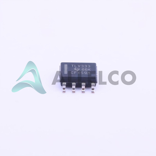
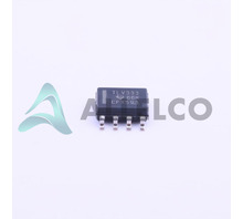
TLV333IDR (1)
Manufacturer Part Number
TLV333IDR
Manufacturer
Texas Instruments
Introduction
The TLV333IDR is a high-performance, low-power operational amplifier (op-amp) from Texas Instruments. It is part of the TLV333 series and designed for use in various instrumentation, measurement, and control applications.
Product Features and Performance
Rail-to-rail input and output
Ultra-low input bias current of 70 pA
Gain bandwidth product of 350 kHz
Slew rate of 0.16V/μs
Input offset voltage of 2 mV
Wide operating voltage range of 1.8V to 5.5V
Wide operating temperature range of -40°C to 125°C
Product Advantages
Excellent precision and stability
Low power consumption
Small 8-SOIC package
Suitable for battery-powered and portable applications
TLV333IDR (2)
Key Technical Parameters
Package: 8-SOIC (0.154", 3.90mm Width)
Mounting Type: Surface Mount
Number of Circuits: 1
Voltage Supply Span (Min): 1.8V
Voltage Supply Span (Max): 5.5V
Current Supply: 17μA
Slew Rate: 0.16V/μs
Voltage Input Offset: 2mV
Amplifier Type: Zero-Drift
Quality and Safety Features
RoHS3 compliant
Reliable and durable performance
Compatibility
This op-amp is compatible with a wide range of electronic circuits and systems, including:
Instrumentation and measurement equipment
Process control and automation
Battery-powered and portable devices
Application Areas
Instrumentation and measurement
Process control and automation
Portable and battery-powered devices
Sensor signal conditioning
Analog-to-digital conversion
Product Lifecycle
The TLV333IDR is an active and widely used product in Texas Instruments' lineup. There are no plans for its discontinuation, and it remains a popular choice for engineers and designers.
Key Reasons to Choose This Product
Excellent precision and stability due to the zero-drift amplifier design
Low power consumption, making it suitable for battery-powered applications
Wide operating voltage and temperature range for versatile use
Small and compact 8-SOIC package for space-constrained designs
RoHS3 compliance for environmentally-friendly applications


 TLV320DAC32IRHBTG4Texas InstrumentsIC DAC 24BIT 96K 32VQFN
 TLV3401CDBVTTexas InstrumentsIC COMPARATOR 1 GEN PUR SOT23-5
 TLV3401CDBVRTexas InstrumentsIC COMPARATOR 1 GEN PUR SOT23-5
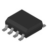 TLV3401CDRTexas InstrumentsSINGLE COMPARATOR
 TLV3401IDTexas Instruments
 TLV3257Freescale / NXP Semiconductors


