
TLV4333IPWR (1)
Manufacturer Part Number
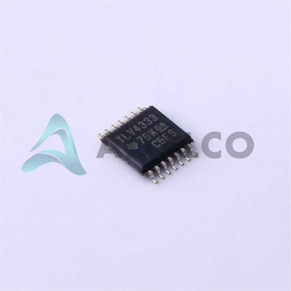
TLV4333IPWR
Manufacturer
Texas Instruments
Introduction
Precision zero-drift operational amplifier
Designed for a wide range of instrumentation and industrial applications
Product Features and Performance
Rail-to-rail input and output
Low input offset voltage of 2 μV
Ultra-low input bias current of 70 pA
High gain bandwidth product of 350 kHz
Slew rate of 0.16 V/μs
Operates from 1.8 V to 5.5 V supply
-40°C to 125°C operating temperature range
Product Advantages
Excellent stability and precision
Extremely low noise and drift
Wide supply voltage range
Suitable for low-power applications
TLV4333IPWR (2)
Key Technical Parameters
Supply voltage range: 1.8 V to 5.5 V
Input offset voltage: 2 μV
Input bias current: 70 pA
Gain bandwidth product: 350 kHz
Slew rate: 0.16 V/μs
Operating temperature range: -40°C to 125°C
Quality and Safety Features
RoHS3 compliant
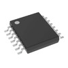
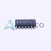
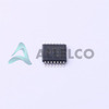
Packaged in a 14-TSSOP (0.173", 4.40mm Width) surface mount package
Compatibility
Compatible with a wide range of instrumentation and industrial applications
Application Areas
Precision instrumentation
Process control equipment
Medical devices
Battery-powered equipment
Product Lifecycle
This product is currently in production and available for purchase
Texas Instruments provides long-term support and availability for this product line
Key Reasons to Choose This Product
Exceptional stability and precision
Ultra-low noise and drift characteristics
Wide supply voltage and temperature range
Ideal for low-power, high-accuracy applications
Robust package and RoHS3 compliance for reliability
 TLV431QPKTexas InstrumentsIC VREF SHUNT ADJ 1.5% SOT89-3
 TLV431TFTADiodes IncorporatedIC VREF SHUNT ADJ 0.2% SOT23
 TLV4906LHALA1Infineon TechnologiesMAGNETIC SWITCH UNIPOLAR SSO-3-2
 TLV493DA1B62GOKITTOBO1Infineon Technologies3D MAGNETICS SENSOR 2GO KIT-TL
 TLV4906KCypress Semiconductor (Infineon Technologies)
 TLV4906LInfineon TechnologiesTLV4906 - HALL SWITCH
 TLV4333IPWTexas Instruments
 TLV431TQFTADiodes IncorporatedIC VREF SHUNT ADJ 0.2% SOT23
 TLV4906KFTSA1Infineon
 TLV431TXFTANA


