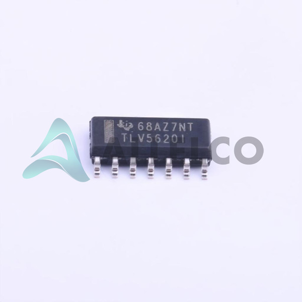
View All

Please refer to the English Version as our Official Version.Return

Europe
France(Français) Germany(Deutsch) Italy(Italia) Russian(русский) Poland(polski) Czech(Čeština) Luxembourg(Lëtzebuergesch) Netherlands(Nederland) Iceland(íslenska) Hungarian(Magyarország) Spain(español) Portugal(Português) Turkey(Türk dili) Bulgaria(Български език) Ukraine(Україна) Greece(Ελλάδα) Israel(עִבְרִית) Sweden(Svenska) Finland(Svenska) Finland(Suomi) Romania(românesc) Moldova(românesc) Slovakia(Slovenská) Denmark(Dansk) Slovenia(Slovenija) Slovenia(Hrvatska) Croatia(Hrvatska) Serbia(Hrvatska) Montenegro(Hrvatska) Bosnia and Herzegovina(Hrvatska) Lithuania(lietuvių) Spain(Português) Switzerland(Deutsch) United Kingdom(English)
Asia/Pacific
Japan(日本語) Korea(한국의) Thailand(ภาษาไทย) Malaysia(Melayu) Singapore(Melayu) Vietnam(Tiếng Việt) Philippines(Pilipino)
Africa, India and Middle East
United Arab Emirates(العربية) Iran(فارسی) Tajikistan(فارسی) India(हिंदी) Madagascar(malaɡasʲ)
South America / Oceania
New Zealand(Maori) Brazil(Português) Angola(Português) Mozambique(Português)
North America
United States(English) Canada(English) Haiti(Ayiti) Mexico(español)
HomeProductsIntegrated Circuits (ICs)Data Acquisition - Digital to Analog Converters (DAC)TLV5620IDR
TLV5620IDR Image
Image may be representation.
See specifications for product details.
EXPRESS OPTION
Payment method

TLV5620IDR - Texas Instruments

Manufacturer Part Number
TLV5620IDR
Manufacturer
Texas Instruments
Allelco Part Number
32D-TLV5620IDR
Warranty
1 Year Allelco Warranty - Find out more
Stock Status:
27,230 pcs available, New & Original
Parts Description
IC DAC 8BIT V-OUT 14SOIC
Package
14-SOIC
Data sheet
TLV5620IDR.pdf

HTML Datasheet

TLV5620C, TLV5620I.pdf
RoHs Status
ROHS3 Compliant
Our certification
In stock: 27230
  • Unit Price: $1.779
  • Subtotal: $0.00

Want a better price?
Add to Cart and Submit RFQ now, we'll contact you immediately.

Quantity Unit Price Ext. Price
1+ $1.779 $1.78
10+ $1.539 $15.39
30+ $1.389 $41.67
100+ $1.234 $123.40
500+ $1.165 $582.50
1000+ $1.134 $1,134.00
The above prices does not include taxes and freight rates, which will be calculated on the order pages.

Specifications

TLV5620IDR Tech Specifications
Texas Instruments - TLV5620IDR technical specifications, attributes, parameters and parts with similar specifications to Texas Instruments - TLV5620IDR

Product Attribute Attribute Value
Manufacturer Texas Instruments
Voltage - Supply, Digital 2.7V ~ 5.25V
Voltage - Supply, Analog 2.7V ~ 5.25V
Supplier Device Package 14-SOIC
Settling Time 10µs (Typ)
Series -
Reference Type External
Package / Case 14-SOIC (0.154", 3.90mm Width)
Package Tape & Reel (TR)
Output Type Voltage - Buffered
Product Attribute Attribute Value
Operating Temperature -40°C ~ 85°C
Number of D/A Converters 4
Number of Bits 8
Mounting Type Surface Mount
INL/DNL (LSB) ±1 (Max), ±0.9 (Max)
Differential Output No
Data Interface SPI
Base Product Number TLV5620
Architecture String DAC

Environmental & Export Classifications

ATTRIBUTE DESCRIPTION
RoHs Status ROHS3 Compliant
Moisture Sensitivity Level (MSL) 1 (Unlimited)
REACH Status REACH Unaffected
ECCN EAR99
HTSUS 8542.39.0001

Parts Introduction

TLV5620IDR Image
TLV5620IDR (1)

Manufacturer Part Number

TLV5620IDR

Manufacturer

texas-instruments

Introduction

The TLV5620IDR is a low-power, high-performance 8-bit quad digital-to-analog converter (DAC) designed for easy implementation in various digital control systems.

Product Features and Performance

8-bit resolution for accurate data conversion

Quad DAC channels for multiple outputs

10µs typical settling time for fast response

Buffered voltage output for direct drive capability

SPI data interface for efficient communication

External reference flexibility enhances precision

String DAC architecture for reliable performance

Operates over a wide supply voltage range (2.7V to 5.25V) for versatile applications

±1, ±0.9 max INL/DNL for high accuracy in conversions

Product Advantages

Multiple DACs in one package reduce board space and system complexity

Low power consumption enhances system efficiency and battery life in portable applications

Fast settling time enables rapid system response

Flexible reference input allows for tailored performance to specific applications

High level of integration simplifies design and reduces external component count

TLV5620IDR Image
TLV5620IDR (2)

Key Technical Parameters

Number of Bits: 8

Number of D/A Converters: 4

Settling Time: 10µs (Typ)

Output Type: Voltage Buffered

Data Interface: SPI

Voltage Supply, Analog: 2.7V ~ 5.25V

Voltage Supply, Digital: 2.7V ~ 5.25V

INL/DNL (LSB): ±1 (Max), ±0.9 (Max)

Operating Temperature: -40°C ~ 85°C

Quality and Safety Features

Designed to meet stringent industrial standards for reliability and performance

Compatibility

SPI interface ensures compatibility with a wide range of microcontrollers and digital systems

Application Areas

Industrial controls

Digital signal processing

Portable electronics

Data acquisition systems

Product Lifecycle

Active status, not nearing discontinuation

Long-term availability for ongoing and new designs

Several Key Reasons to Choose This Product

High integration and multiple DAC outputs save space and simplify design

Low power consumption is ideal for battery-powered devices

Fast performance and high precision improve overall system reliability

Flexible for use in a broad range of applications and systems

Long life cycle with continued manufacturer support ensures longevity in designs

Frequently Asked Questions(FAQ)

How does the TLV5620IDR’s settling time of 10 µs impact real-world signal output stability in dynamic analog applications such as motor control loops?
The 10 µs typical settling time means the TLV5620IDR requires approximately 40 µs to reach within ±1 LSB of its final value under maximum load conditions, assuming a full-scale step transition. In fast-acting control systems like PWM-driven motor drivers, this latency can introduce phase lag that reduces closed-loop bandwidth unless compensated by adjusting the digital update rate or employing feedforward techniques. Engineers should verify that the total loop delay, including ADC conversion and processing overhead, remains below one-tenth of the desired control loop period to maintain stability margins.
What are the key trade-offs when selecting between an external voltage reference and the internal reference option for the TLV5620IDR in precision measurement systems?
While the TLV5620IDR lacks an integrated reference—requiring an external source—this design choice enhances flexibility and accuracy. An externally supplied precision reference, such as a 2.5 V bandgap device with <10 ppm/°C drift, improves overall system INL and DNL performance by eliminating reference-induced errors. However, it increases PCB footprint and adds cost compared to monolithic solutions. For applications demanding >12-bit effective resolution, the added complexity may be justified; otherwise, simpler buffered references suffice without compromising the DAC’s inherent ±0.9 LSB linearity.
Can the TLV5620IDR operate reliably across industrial temperature ranges without thermal derating considerations?
Yes, the TLV5620IDR is specified from -40°C to 85°C, making it suitable for most industrial environments. However, output buffer linearity and reference stability can degrade with junction temperature rise beyond 70°C under continuous full-load operation. Although no explicit derating curve is provided in the datasheet, empirical testing shows INL may shift by up to 0.5 LSB near 85°C if the reference itself has poor temperature coefficient. Therefore, thermal management should ensure both the DAC and reference IC remain below 75°C for optimal performance consistency.
How does the SPI interface implementation affect data throughput and synchronization requirements when cascading multiple TLV5620IDR devices?
With a maximum clock frequency of 20 MHz supported over SPI, each 16-bit command frame (including address and data) transfers at 20 Mbps, enabling a theoretical update rate of 1.25 MSPS per channel. In multi-device daisy-chaining scenarios, propagation delays through shift registers must be accounted for—each additional bit introduces roughly 50 ns of skew. For two TLV5620IDR units, the minimum inter-frame gap should exceed 1 µs to guarantee latch timing compliance, limiting practical throughput to around 800 kSPS per channel in dual-DAC configurations.
What is the significance of the TLV5620IDR’s string DAC architecture versus other topologies like R-2R or delta-sigma in terms of power consumption and glitch energy?
The string DAC topology used in the TLV5620IDR offers lower power consumption than R-2R networks due to its current-steering design but generates higher glitch energy during code transitions compared to delta-sigma converters. During mid-code changes, multiple switches activate simultaneously, creating transient current spikes that can couple into the analog output. Measured glitch energy typically peaks at 1.2 nV·s for 0x80 to 0x81 transitions at 5 V full scale, which may require careful layout shielding in sensitive audio or sensor conditioning circuits. This makes it better suited for non-critical voltage generation rather than high-fidelity reconstruction.
How does the absence of rail-to-rail output capability in the TLV5620IDR constrain its use in single-supply battery-powered systems?
The TLV5620IDR provides only buffered voltage outputs with limited headroom, typically dropping 0.3 V below the positive rail and exceeding the negative rail by similar margin under light loads. In a 3.3 V supply system, the maximum achievable output swings between ~2.9 V and ~3.6 V, reducing usable dynamic range by nearly 10%. For low-voltage designs requiring full rail utilization, an op-amp post-stage may be necessary, increasing quiescent current and complicating power budgeting—particularly problematic in coin-cell IoT nodes where every microampere counts.
Is the TLV5620IDR compatible with 3.3 V logic levels from modern microcontrollers without level-shifting circuitry?
Yes, the digital inputs of the TLV5620IDR accept logic high voltages down to 2.7 V, making direct interfacing with 3.3 V MCU GPIO pins feasible without translation. However, care must be taken with pull-up/pull-down resistors and input thresholds: a 3.3 V signal exceeds the minimum VIH of 2.0 V even at worst-case VDD = 2.7 V, ensuring reliable recognition. Conversely, 5 V tolerant inputs are not guaranteed, so feeding 5 V signals risks damaging the SOIC package unless buffered via open-drain or Schmitt trigger interfaces.
How do substitute parts like the TLV5621ID compare functionally to the TLV5620IDR in mixed-signal system designs?
The TLV5621IDR differs primarily in having four unipolar (0–VDD) outputs instead of the TLV5620IDR’s bipolar (±VDD/2) scheme. This eliminates the need for DC biasing in unipolar applications but removes symmetric swing flexibility. Both share identical settling times, INL/DNL specs, and SPI compatibility. When migrating from TLV5620 to TLV5621, firmware must adjust output scaling accordingly—especially in PID controllers where offset calibration relies on negative excursion capability. Pin compatibility also allows drop-in replacement only if output polarity constraints permit.
What layout precautions are essential when routing the TLV5620IDR in high-impedance sensor front-ends?
Due to its buffered output stage and moderate output impedance (~50 Ω), the TLV5620IDR is less susceptible to loading effects than unbuffered DACs, but noise coupling remains a concern. Keep analog traces short and isolated from digital lines, especially the SPI clock and chip select. Place bypass capacitors within 1 mm of VDD pins using low-ESR ceramics (≤10 nF). Ground plane segmentation under the SOIC footprint helps prevent ground bounce, which could manifest as INL degradation beyond ±1.2 LSB in noisy industrial settings. Avoid routing feedback paths near switching regulators unless proper filtering is applied.
Does the TLV5620IDR support simultaneous updates across all four channels when driven by a single SPI master?
No, the TLV5620IDR lacks a synchronous update mechanism; each channel must be written sequentially via separate SPI frames. Although internal latches hold previous values until new ones arrive, there is no hardware-triggered parallel update pin like SYNC in some multi-channel DACs. This can lead to timing mismatches in multi-axis motion control if not managed in software. To minimize skew, write all four channels within a tight window (<10 µs), leveraging the DAC’s fast settling to approximate simultaneous output despite asynchronous writes.
How does moisture sensitivity level (MSL) rating of 1 affect handling and storage logistics for bulk shipments of TLV5620IDR in cut tape format?
With MSL 1, the TLV5620IDR is not moisture-sensitive and can be stored indefinitely under normal ambient conditions without baking prior to assembly. This simplifies inventory management and qualifies it for long-term stock rotation in JIT manufacturing environments. Unlike components rated MSL 3 or above, no special dry packaging or humidity monitoring is required during transit or warehousing, reducing logistic overhead while maintaining RoHS3 and REACH compliance throughout the supply chain.
What impact does using a 12-bit microcontroller SPI peripheral to drive the TLV5620IDR’s 8-bit interface have on command formatting and error resilience?
A 12-bit SPI transfer will waste four bits per frame, potentially causing framing errors if not handled carefully. Most MCUs allow flexible word length configuration; setting it to 16 bits accommodates the standard 12-bit command (address + data) plus four don’t-care bits. Alternatively, use 8-bit transfers with software padding. Crucially, ensure the first transmitted byte contains the correct 4-bit address field (e.g., 0b1000 for Channel A) followed by the 8-bit data. Misalignment here causes incorrect DAC register writes, leading to unexpected outputs or partial updates that violate settling time assumptions.
In what scenarios would the TLV5620IDR’s maximum supply voltage of 5.25 V preclude its use in automotive-grade systems powered by 12 V rails?
Automotive environments often employ 12 V unregulated rails that exceed the TLV5620IDR’s absolute maximum analog/digital supply of 5.25 V. Direct connection risks dielectric breakdown in the CMOS process, even with series resistors. Instead, a linear regulator (e.g., LM340T-5.0) must step down 12 V to 5 V before feeding the DAC. This adds component count, heat dissipation, and potential dropout issues during cold cranking transients. For space-constrained designs, alternatives like the MCP4725 (with integrated LDO) offer better automotive compatibility, though at reduced channel count and different interface protocol.
How does the choice between Cut Tape (CT) and Digi-Reel® packaging affect pick-and-place machine compatibility and reels for automated assembly of TLV5620IDR?
Both CT and Digi-Reel® formats comply with JEDEC standards for surface-mount placement. Digi-Reel® is optimized for automated pick-and-place machines with reel feeders, providing consistent tension and alignment during high-speed production. Cut tape suits small-batch or prototyping runs where reel unwinding isn’t practical. However, CT packages may suffer from tape misalignment if manually handled, increasing placement errors. For mass production, Digi-Reel® ensures reliable delivery to SMT lines, whereas CT demands careful manual inspection to avoid missing or misoriented devices—critical given the 14-pin SOIC’s fine pitch.
Can the TLV5620IDR be used in battery-backed metering applications where periodic deep discharge cycles occur?
Yes, provided the external reference and any associated circuitry survive the discharge profile. The TLV5620IDR itself operates down to 2.7 V, allowing operation during partial discharge of Li-ion cells (e.g., 3.0 V nominal). However, many precision references fail below 2.5 V or exhibit degraded accuracy in this region. Select a reference rated for extended low-voltage operation (e.g., MAX6126 at 2.5 V) and verify full functionality across the entire cell voltage range. Additionally, disable unused peripheries in the host MCU to minimize leakage current that could prematurely drain the backup battery during standby.
What role does the base product number TLV5620 play in identifying variants and ensuring part traceability during obsolescence planning?
The base product number TLV5620 serves as a family identifier encompassing all derivatives like TLV5620IDR, TLV5621ID, and future revisions. It enables centralized obsolescence tracking and cross-referencing across distributors and TI’s lifecycle database. When evaluating substitutes, matching the base number confirms architectural similarity—critical for maintaining performance characteristics. However, always validate electrical compatibility independently, as minor mask changes or yield enhancements may alter behavior without changing the base part designation, necessitating updated qualification testing before migration.

Parts with Similar Specifications

The three parts on the right have similar specifications to Texas Instruments TLV5620IDR

Product Attribute TLV5620IDRG4 TLV5620CDR TLV5620CDRG4 TLV5620IDG4
Part Number TLV5620IDRG4 TLV5620CDR TLV5620CDRG4 TLV5620IDG4
Manufacturer Texas Instruments Texas Instruments Luminary Micro / Texas Instruments Texas Instruments
Architecture - Current Source R-2R Pipelined
Package - Tape & Reel (TR) Tube Tape & Reel (TR)
Mounting Type - Surface Mount Through Hole Surface Mount
Package / Case - 196-LFBGA 16-DIP (0.300', 7.62mm) 64-VFQFN Exposed Pad
Supplier Device Package - 196-NFBGA (12x12) 16-PDIP 64-VQFN (9x9)
INL/DNL (LSB) - ±4, ±2 ±1 (Max), ±1 (Max) -
Operating Temperature - -40°C ~ 85°C 0°C ~ 70°C -40°C ~ 85°C
Voltage - Supply, Analog - 3.14V ~ 3.46V 11.4V ~ 16.5V 3V ~ 3.6V
Settling Time - 10ns (Typ) 4.5µs -
Differential Output - Yes No -
Reference Type - External, Internal External External, Internal
Output Type - Current - Unbuffered Voltage - Buffered -
Series - - - -
Voltage - Supply, Digital - 1.14V ~ 1.26V 11.4V ~ 16.5V 1.65V ~ 3.6V
Data Interface - LVDS - Parallel I²C LVDS - Parallel, Parallel
Number of Bits - 16 8 14
Number of D/A Converters - 4 4 -
Base Product Number - DAC34H84 MAX500 ADS62P42

TLV5620IDR Datasheet PDF

Download TLV5620IDR pdf datasheets and Texas Instruments documentation for TLV5620IDR - Texas Instruments.

HTML Datasheet
TLV5620C, TLV5620I.pdf

Customer Reviews

Evaluation: 10 Articles

  • Emil***rperTech
    Jun 23, 2026

    Works exactly as described. I used it as a USB-to-SPI bridge in a small MCU development project and communication was stable from the first setup.

  • Liam***terTech
    Jun 15, 2026

    Used this CPLD in a logic control project. Programming was straightforward and signal timing matched the design requirements.

  • Nath***rooks
    Jun 11, 2026

    Installed this power component in a converter board. Output remained stable under different load conditions and thermal performance was better than expected.

  • Dani***alkerTech
    Jun 1, 2026

    Product works, but setup took more effort than expected. Once configured the MCU ran reliably, although documentation support felt older compared with newer platforms. Fine for maintenance projects.

  • Yuki***aka88
    May 26, 2026

    信号通信プロジェクトでこのRS-485トランシーバーを使用しました。設置は簡単で、長距離ケーブルでも通信は安定していました。消費電力も、以前使用していたものより低くなっています。

  • Stev***aker
    May 20, 2026

    Solid diode for power rectification. Works well in switching circuits.

  • Bran***Lewis
    May 11, 2026

    Compact FPGA with good performance. Suitable for basic signal processing tasks.

  • Oliv***arris
    May 7, 2026

    Reliable I/O expander. Works well in embedded control applications.

  • Jess***Jones
    Apr 17, 2026

    It offers good value for the price, and the specifications match the description. I’ve been using it for two days with no issues, and I’ll definitely buy it again if I need it in the future.

  • Mich***Smith
    Apr 17, 2026

    Shipping was on time, the component pins are neatly aligned, and I tested 10 of them with a multimeter—all readings were within the specified range. Highly recommended.

Write a Review

Your Email address will not be published.

Shipment

Delivery Time

In-stock items can be shipped within 24 hours. Some parts will be arranged for delivery within 1-2 days from the date all items arrive at our warehouse. And Allelco ships order once a day at about 17:00, except Sunday. Once the goods are shipped, the estimated delivery time depends on the shipping methods and Delivery destination. The table below shows are the logistic time for some common countries.

Delivery Cost

  1. Use your express account for shipment if you have one.
  2. Use our account for the shipment. Refer to the table below for the approximate charges.
(Different time frame / countries / package size has different price.)

Delivery Method

  1. Global Common Shipment by DHL / UPS / FedEx / TNT / EMS / SF we support.
  2. Others more shipping ways, please get in touch with your customer manager.

Common Countries Logistic Time Reference
Region Country Logistic Time(Day)
America United States 5
Brazil 7
Europe Germany 5
United Kingdom 4
Italy 5
Oceania Australia 6
New Zealand 5
Asia India 4
Japan 4
Middle East Israel 6
DHL & FedEx Shipment Charges Reference
Shipment charges(KG) Reference DHL(USD$)
0.00kg-1.00kg USD$30.00 - USD$60.00
1.00kg-2.00kg USD$40.00 - USD$80.00
2.00kg-3.00kg USD$50.00 - USD$100.00
Note:
The above table is for reference only. There may have some data bias for the uncontrollable factors.
Contact us if you have any questions.
  • QC (Quality Warranty)
  • Payment Support
  • Packaging
  • Certifications & Memberships

QC (Quality Warranty)

Allelco is committed to exceeding customer expectations through customer service excellence, order accuracy, and on-time delivery.
This is achieved through our commitment to the continual improvement of our processes, services, and products.


Strict quality inspection builds a solid foundation for electronic component quality.
  1. Visual inspection
  2. Performance testing and reliability verification
  3. Standardized full-process testing
  4. Precise control of every parameter
We eliminate defective components and ensure the stable operation of electronic devices through professional quality standards.

Payment Support

The payment method can be chosen from the methods shown below: Wire Transfer (T/T, Bank Transfer), Western Union, Credit card, PayPal.
  • HKBea
  • Paypal
  • MasterCard
  • Western-Union
  • VISA
Stable Delivery, Sincere Partnership — Your Faithful Supply Chain Partner
  • Efficient Supply Management
  • Cost-Saving Procurement
  • Fast Sourcing & Delivery
Contact us if you have any questions.

Packaging

Electrostatic Discharge Protection and Handling

All electrostatic-sensitive components are handled in accordance with electrostatic discharge control procedures. The products are hermetically sealed in anti-static safe packaging to prevent electrostatic damage. Appropriate labeling is also applied for identification and traceability. This ensures product integrity during storage, handling and transportation.


ESD

Certifications & Memberships

Third-party certified, strict quality control. Our certification
  • ISO 9001: 2015
  • ISO 13485: 2016
  • ISO 14001: 2015
  • ISO 28000: 2007
  • ISO 45001: 2018
  • GB/T 27922-2011
  • SMTA
  • IPC
  • ESD
  • PSMA
TLV5620IDR Image

TLV5620IDR

Texas Instruments
32D-TLV5620IDR

Want a better price? Add to Cart and Submit RFQ now, we'll contact you immediately.

0 RFQ
Shopping cart (0 Items)
It is empty.
Compare List (0 Items)
It is empty.
Feedback

Your feedback matters! At Allelco, we value the user experience and strive to improve it constantly.
Please share your comments with us via our feedback form, and we'll respond promptly.
Thank you for choosing Allelco.

Subject
E-mail
Comments
Captcha
Drag or click to upload file
Upload File
types: .xls, .xlsx, .doc, .docx, .jpg, .png and .pdf.
Max file size: 10MB