TPS2557DRBT (1)
Manufacturer Part Number
TPS2557DRBT
Manufacturer
Texas Instruments
Introduction
Precision Adjustable Current-Limited Power-Distribution Switch
Product Features and Performance
Precision current limiting
Adjustable current-limit threshold
Slew rate controlled load switching
On/Off control via digital input
Automatic retry fault management
Status flag for fault indication
Thermal shutdown protection
Reverse voltage blocking
Under-voltage lockout (UVLO)
Product Advantages
Highly accurate current limit (±10% at 1.5A)
Low Rds(on) for higher efficiency and lower heat dissipation
Supports 2.5V to 6.5V voltage range
Capable of supplying up to 5A continuous current
Robust thermal performance with operating temperature from -40°C to 125°C
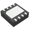
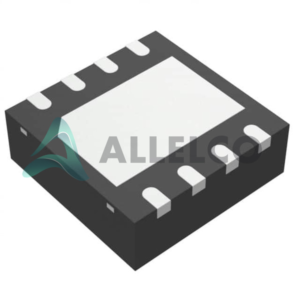
Small form factor with 8-SON (3x3) package

TPS2557DRBT (2)
Key Technical Parameters
Output Current (Max): 5A
Rds On (Typical): 22mOhm
Voltage - Load: 2.5V – 6.5V
Number of Outputs: 1
Output Configuration: High Side
Input Type: Non-Inverting
Quality and Safety Features
Current Limiting (Adjustable)
Over Temperature Protection
Under-Voltage Lock Out
Compatibility
General compatibility with a wide range of microcontrollers and digital systems due to non-inverting On/Off interface
Application Areas
USB ports and hubs
Hot-swap power supplies
Industrial controls
Peripheral power management
Portable and battery-powered equipment
Product Lifecycle
Active status
Not impending discontinuation
Replacements or upgrades are available if necessary
Several Key Reasons to Choose This Product
Accurate control of current for system reliability
Adjustability of current limit provides flexibility in application use
Highly efficient power distribution minimizing system losses
Built-in safety features ensure protection against fault conditions
Versatile compatibility with different systems and applications
Extended operating temperature range suitable for harsh environments
Reliable power management solution from a reputable manufacturer


 TPS2560ADRCRTexas InstrumentsIC PWR SWITCH N-CHAN 1:2 10VSON
 TPS2557DRBEVM-423Texas InstrumentsEVAL MODULE FOR TPS2557DRB-423
 TPS2559DRCTTexas InstrumentsIC PWR SWITCH N-CHAN 1:1 10VSON
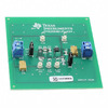 TPS2559EVM-624Texas InstrumentsEVAL MODULE FOR TPS2559
 TPS2556QDRBRQ1Texas InstrumentsIC PWR SWITCH N-CHAN 1:1 8SON
 TPS2556DRBRTexas InstrumentsIC PWR SWITCH N-CHAN 1:1 8SON
 TPS2559DRCRTexas InstrumentsIC PWR SWITCH N-CHAN 1:1 10VSON
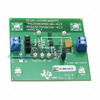 TPS2556DRBEVM-423Texas InstrumentsEVAL MODULE FOR TPS2556DRB-423


