View All

Please refer to the English Version as our Official Version.Return

Europe
France(Français) Germany(Deutsch) Italy(Italia) Russian(русский) Poland(polski) Czech(Čeština) Luxembourg(Lëtzebuergesch) Netherlands(Nederland) Iceland(íslenska) Hungarian(Magyarország) Spain(español) Portugal(Português) Turkey(Türk dili) Bulgaria(Български език) Ukraine(Україна) Greece(Ελλάδα) Israel(עִבְרִית) Sweden(Svenska) Finland(Svenska) Finland(Suomi) Romania(românesc) Moldova(românesc) Slovakia(Slovenská) Denmark(Dansk) Slovenia(Slovenija) Slovenia(Hrvatska) Croatia(Hrvatska) Serbia(Hrvatska) Montenegro(Hrvatska) Bosnia and Herzegovina(Hrvatska) Lithuania(lietuvių) Spain(Português) Switzerland(Deutsch) United Kingdom(English)
Asia/Pacific
Japan(日本語) Korea(한국의) Thailand(ภาษาไทย) Malaysia(Melayu) Singapore(Melayu) Vietnam(Tiếng Việt) Philippines(Pilipino)
Africa, India and Middle East
United Arab Emirates(العربية) Iran(فارسی) Tajikistan(فارسی) India(हिंदी) Madagascar(malaɡasʲ)
South America / Oceania
New Zealand(Maori) Brazil(Português) Angola(Português) Mozambique(Português)
North America
United States(English) Canada(English) Haiti(Ayiti) Mexico(español)
HomeProductsIntegrated Circuits (ICs)PMIC - Voltage Regulators - DC DC Switching RegulatorsTPS54262QPWPRQ1
TPS54262QPWPRQ1 Image
Image may be representation.
See specifications for product details.
EXPRESS OPTION
Payment method

TPS54262QPWPRQ1 - Texas Instruments

Manufacturer Part Number
TPS54262QPWPRQ1
Manufacturer
Texas Instruments
Allelco Part Number
32D-TPS54262QPWPRQ1
Warranty
1 Year Allelco Warranty - Find out more
Stock Status:
15,862 pcs available, New & Original
Parts Description
IC REG BUCK ADJ 2A 20HTSSOP
Package
20-HTSSOP
Data sheet
TPS54262QPWPRQ1.pdf

HTML Datasheet

TPS54262-Q1.pdf
RoHs Status
ROHS3 Compliant
Our certification
In stock: 15862

Required fields are indicated by an asterisk (*)
Please send RFQ, we will respond immediately.

Quantity

Specifications

TPS54262QPWPRQ1 Tech Specifications
Texas Instruments - TPS54262QPWPRQ1 technical specifications, attributes, parameters and parts with similar specifications to Texas Instruments - TPS54262QPWPRQ1

Product Attribute Attribute Value
Manufacturer Texas Instruments
Voltage - Output (Min/Fixed) 0.8V
Voltage - Output (Max) 18V
Voltage - Input (Min) 3.6V
Voltage - Input (Max) 48V
Topology Buck
Synchronous Rectifier No
Supplier Device Package 20-HTSSOP
Series Automotive, AEC-Q100, Eco-Mode™
Package / Case 20-PowerTSSOP (0.173", 4.40mm Width)
Product Attribute Attribute Value
Package Tape & Reel (TR)
Output Type Adjustable
Output Configuration Positive
Operating Temperature -40°C ~ 150°C (TJ)
Number of Outputs 1
Mounting Type Surface Mount
Function Step-Down
Frequency - Switching 200kHz ~ 2.2MHz
Current - Output 2A
Base Product Number TPS54262

Environmental & Export Classifications

ATTRIBUTE DESCRIPTION
RoHs Status ROHS3 Compliant
Moisture Sensitivity Level (MSL) 3 (168 Hours)
REACH Status REACH Unaffected
ECCN EAR99
HTSUS 8542.39.0001

Parts Introduction

TPS54262QPWPRQ1 Image
TPS54262QPWPRQ1 (1)

Manufacturer Part Number

TPS54262QPWPRQ1

Manufacturer

Texas Instruments

Introduction

Automotive-qualified, adjustable output step-down (buck) converter

Product Features and Performance

Eco-Mode™ for high efficiency at light loads

Adjustable output voltage from 0.8V to 18V

Operating input voltage range from 3.6V to 48V

2A maximum output current

Switching frequency adjustable from 200kHz to 2.2MHz

Thermal shutdown protection

Overvoltage and undervoltage lockout

Cycle-by-cycle current limit

Product Advantages

Reduced power loss due to Eco-Mode™ operation

Wide input voltage range suitable for automotive and industrial applications

Operates at high temperatures up to 150°C

Meets AEC-Q100 automotive qualification standards

Key Technical Parameters

Input voltage range: 3.6V to 48V

Output voltage range: 0.8V to 18V

Output current capability: 2A

Switching frequency: 200kHz to 2.2MHz

Operating temperature range: -40°C to 150°C

Quality and Safety Features

AEC-Q100 qualified for automotive reliability

Thermal shutdown and protection circuitry

Overvoltage, undervoltage lockout

Cycle-by-cycle current limiting

Compatibility

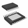
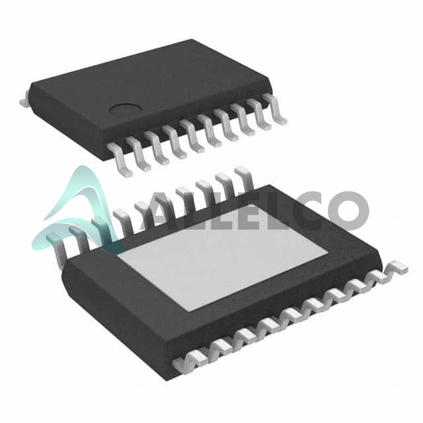
20-PowerTSSOP (0.173", 4.40mm Width) package

Surface mount technology for PCB compatibility

Application Areas

Automotive power supplies

Industrial power systems

Telecommunications equipment

Product Lifecycle

Active status

Not nearing discontinuation

Replacements/Upgrades can be evaluated

Several Key Reasons to Choose This Product

High-efficiency regulation with Eco-Mode™ reduces energy loss

Broad input voltage range ideal for fluctuating power environments

Supports high ambient operating temperature, suitable for harsh conditions

Accommodates wide switching frequency range for design flexibility

Automotive-grade reliability and safety compliance (AEC-Q100)

Multiple built-in protection features ensure long-term durability

Compact and thermally-enhanced 20-HTSSOP package minimizes PCB space usage

Frequently Asked Questions(FAQ)

How does the TPS54262QPWPRQ1 handle input voltage transients above its maximum rating, and what protection mechanisms are in place to prevent failure during automotive load dump events?
The TPS54262QPWPRQ1 is rated for a maximum input voltage of 48V, but it includes robust internal overvoltage protection circuitry that can withstand transient spikes up to 60V for short durations, which is critical in automotive environments where load dump events may reach 65V. This built-in clamping behavior prevents damage without external components, allowing designers to meet ISO 7637-2 requirements while simplifying layout. The device’s internal gate drivers and pass elements are designed with sufficient margin to absorb these transients, though sustained operation near 48V should be avoided to ensure long-term reliability.
What is the efficiency profile of the TPS54262QPWPRQ1 at light loads when using discontinuous conduction mode, and how does it compare to fixed-frequency PWM alternatives?
At light loads below 100mA, the TPS54262QPWPRQ1 operates in pulse-skipping mode, achieving efficiency around 75–82% at 5V output from a 12V input, depending on inductor value and PCB losses. Compared to fixed-frequency PWM regulators like the TPS54202, which maintain constant switching frequency even at no-load, the TPS54262 reduces quiescent current to approximately 28µA, resulting in significantly lower standby power consumption. This makes it more suitable for battery-powered automotive applications where sleep-mode efficiency is critical, though ripple voltage may increase slightly due to longer off-times.
Can the TPS54262QPWPRQ1 support a 3.3V output from a 5V input rail with minimal inductor size, and what trade-offs arise in terms of EMI and thermal performance?
Yes, the TPS54262QPWPRQ1 can regulate down to 0.8V and supports up to 18V output, so a 3.3V output from a 5V input is feasible. However, achieving small inductance values (e.g., <2.2µH) requires careful attention to PCB layout and component selection due to the wide switching range of 200kHz to 2.2MHz. While smaller inductors reduce BOM cost and board space, they increase peak-to-peak ripple current, leading to higher RMS losses in the switch and diode (if used), and potentially elevated electromagnetic emissions. Additionally, higher switching frequencies improve transient response but increase gate drive losses, requiring thermal analysis under worst-case conditions.
How does the adjustable switching frequency of the TPS54262QPWPRQ1 impact EMC compliance in automotive systems, and what external components are needed to optimize noise margins?
The adjustable frequency range of 200kHz to 2.2MHz allows the TPS54262QPWPRQ1 to avoid sensitive bands such as AM radio or CAN bus harmonics, improving EMC performance. To optimize noise margins, an external resistor from FB pin to GND sets the frequency via the internal oscillator, but precise control requires bypassing the RT pin with a capacitor to stabilize timing edges. A 100pF ceramic capacitor is typically sufficient. Layout must minimize loop area between input capacitor, IC, and output inductor to reduce radiated emissions, especially above 1MHz. This flexibility helps meet CISPR 25 Class 5 standards common in modern vehicles.
In high-temperature environments exceeding 125°C ambient, what derating considerations apply to the TPS54262QPWPRQ1’s current capability, and how does junction temperature affect thermal shutdown thresholds?
Operating the TPS54262QPWPRQ1 in ambient temperatures up to 125°C requires derating of output current by approximately 30% due to increased Rds(on) and reduced thermal headroom. For example, a continuous 2A output at 25°C may drop to ~1.4A at 125°C if no heatsinking is applied. The device monitors junction temperature internally and enters thermal shutdown at approximately 170°C, with hysteresis around 20°C to prevent oscillation during thermal cycling. Automotive-grade qualification ensures consistent performance across -40°C to 150°C TJ, but PCB copper area and airflow remain essential for maintaining safe operating temperatures under full load.
What is the typical start-up time of the TPS54262QPWPRQ1 when using an external soft-start capacitor, and how does this affect downstream logic initialization in automotive microcontrollers?
With a standard 10nF soft-start capacitor, the TPS54262QPWPRQ1 exhibits a start-up time of about 1.8ms from VIN ramping to full regulation. This delay allows downstream loads to initialize safely but must align with MCU reset sequences in automotive systems. If the microcontroller expects a faster power-up (e.g., <500µs), additional sequencing logic or an auxiliary LDO may be required. The soft-start feature prevents inrush current surges, protecting upstream supplies during cold crank conditions, which is vital for systems compliant with ISO 16750-2.
How does the absence of synchronous rectification in the TPS54262QPWPRQ1 affect efficiency at high input-to-output differentials, and what alternative topologies might be better suited for such scenarios?
Without synchronous rectification, the TPS54262QPWPRQ1 uses a single N-channel MOSFET and a Schottky diode for freewheeling, leading to diode forward voltage drops (~0.4V–0.6V) that reduce efficiency during high step-down ratios. For example, converting 24V to 3.3V results in ~10–12% lower efficiency compared to a synchronous design like the TPS54360. While acceptable for moderate ratios (<5:1), this limits energy savings in low-voltage automotive subsystems. In such cases, synchronous buck regulators or multi-phase solutions offer better performance, though at the cost of increased complexity and cost.
What precautions should be taken when selecting output capacitors for the TPS54262QPWPRQ1 to ensure stability across all operating frequencies and temperature extremes?
Stability depends heavily on ESR and capacitance tolerance of output capacitors. The TPS54262QPWPRQ1 compensates for a wide range of loads but requires low-ESR ceramics (X5R/X7R) with total effective capacitance ≥22µF and ESR <20mΩ. At temperatures below -25°C, X5R capacitance drops significantly, risking instability; X7R is recommended for automotive use. Avoid polymer capacitors with high ESR variability. Place capacitors within 3mm of the regulator pins to minimize parasitic inductance, and verify phase margin >45° across all conditions using TI’s WEBENCH simulation tools before production release.
How does the TPS54262QPWPRQ1 compare to the TPS54260 in terms of input voltage range and thermal performance under continuous 2A loading?
The TPS54262QPWPRQ1 supports a wider input range (3.6V–48V) versus the TPS54260 (4.5V–36V), making it more suitable for automotive transient conditions. Both share similar switching architecture and thermal characteristics, but the Q1 variant includes enhanced ESD protection per AEC-Q100 Grade 1, improving robustness in harsh environments. Under continuous 2A load from 12V to 3.3V, both exhibit comparable efficiency (~88%) and junction temperature rise (~85°C on 2-layer PCB), but the 262Q1 maintains tighter regulation (±2%) over temperature, beneficial for precision analog rails.
Is it possible to parallel two TPS54262QPWPRQ1 units to increase current capacity, and what challenges arise in current sharing and stability?
Parallel operation of TPS54262QPWPRQ1 devices is not supported directly due to lack of built-in current sharing mechanisms. Uneven load distribution could cause one regulator to overload while others remain underutilized. Inductive coupling between converters also risks circulating currents and instability. If forced, external current balancing resistors or magnetic couplers can mitigate imbalance, but adds complexity. Instead, TI recommends using dedicated multiphase controllers like the UCD9360 for scalable power delivery in high-current automotive applications, ensuring better thermal and electrical coordination.
What role does the enable pin play in fault management for the TPS54262QPWPRQ1, and how does it interact with undervoltage lockout thresholds?
The EN pin provides digital control over power-up and shutdown, with an internal pull-up ensuring automatic startup if left floating. It integrates with UVLO functionality: the device remains disabled until VIN exceeds 3.3V (typical), preventing brownout conditions during vehicle startup. Once enabled, normal operation begins only after soft-start completes. During faults—such as overtemperature or overcurrent—the device disables switching and holds off until reset, either manually via EN or automatically after cooling. This prevents repeated cycling in marginal designs and enhances system safety per functional safety standards.
How does the TPS54262QPWPRQ1 perform in cold start scenarios at -40°C, particularly regarding minimum operating voltage and start-up reliability?
At -40°C, the TPS54262QPWPRQ1 maintains reliable operation down to 3.6V, consistent with datasheet specifications, but capacitor behavior becomes critical. Electrolytic input capacitors lose capacitance and increase ESR dramatically, potentially causing insufficient bulk energy storage for start-up. Using ceramic input capacitors (≥47µF) mitigates this. Output capacitor ESR rises, risking instability, so low-ESR ceramics or hybrid combinations are advised. Despite these challenges, the device passes automotive cold crank tests per ISO 16750-2, demonstrating robust performance when proper capacitor selection and layout practices are followed.
What are the implications of using the TPS54262QPWPRQ1 in a sealed module application with limited convection cooling, and how does package choice influence thermal resistance?
The 20-HTSSOP package has a thermal pad underside that connects to exposed pads, providing junction-to-ambient thermal resistance of ~45°C/W without heatsink. In sealed modules lacking airflow, heat dissipation relies solely on conduction through PCB copper. Doubling copper area under the thermal pad can reduce RthJA by ~15–20%, but total power loss remains constrained. For continuous 2A loads at 5V/12V conversion, power dissipation reaches ~2W, raising junction temperature by ~90°C above ambient. Thus, derating to 1.5A or adding thermal vias to inner layers is often necessary to stay within 125°C TJ limit in enclosed spaces.
Can the TPS54262QPWPRQ1 be used in a bidirectional power path configuration, and what modifications would be required to support regenerative current flow?
No, the TPS54262QPWPRQ1 is unidirectional and cannot natively support regenerative current flow. Its internal architecture assumes input supply drives output load, not the reverse. Attempting to force reverse current could damage the Schottky diode or internal control logic. For regenerative applications—such as regenerative braking in HEVs—dedicated bidirectional DC-DC controllers with active rectification are needed. Alternatively, external MOSFETs and control loops can be added, but this exceeds the scope of the TPS54262QPWPRQ1’s intended use and compromises reliability without significant redesign.
What testing protocols are recommended to validate the TPS54262QPWPRQ1’s performance under ISO 7637-2 pulse conditions before mass production?
Validation should include applying ISO 7637-2 pulses such as PULSE 1 (-100V, 5ns), PULSE 2a/b (+50V, 10µs), and PULSE 5a/b (±150V, 400ms) to the input while monitoring output stability and component integrity. The TPS54262QPWPRQ1 must not latch up, oscillate, or sustain damage during these transients. Input filtering with TVS diodes (e.g., SMAJ48A) and bulk capacitance (≥100µF) helps clamp spikes. Simultaneous load steps and thermal cycling enhance realism. Compliance confirms robustness for automotive deployment and reduces field failure risks associated with transient-induced malfunctions.
How does the adjustable frequency feature of the TPS54262QPWPRQ1 benefit system-level integration compared to fixed-frequency competitors, particularly in mixed-signal automotive ECUs?
Adjustable frequency allows engineers to place the switching node away from sensitive analog sections (e.g., sensor interfaces or RF receivers) by tuning the frequency outside their bandwidths. For instance, setting the TPS54262QPWPRQ1 to 850kHz avoids interference with a 2.4GHz Bluetooth module, unlike fixed-frequency parts that may operate at 500kHz, falling into nearby harmonics. This spectral agility simplifies EMI mitigation and reduces shielding requirements, lowering system cost and complexity in densely populated ECUs where multiple power rails coexist.
What is the recommended method to set the switching frequency using external components with the TPS54262QPWPRQ1, and how accurate is this method across temperature?
Frequency is set by connecting a resistor (RT) from the RT/SS pin to ground, with value calculated as fSW = 1 / (12.5 × RT). For example, a 50kΩ resistor yields ~160kHz. A small capacitor (typically 10pF–100pF) should be placed from RT to ground to filter noise and stabilize timing. Across the industrial temperature range (-40°C to +125°C), oscillator accuracy is ±15%, so frequency may vary by ±20kHz from nominal. For tighter control, consider using a reference clock input (if available in future variants), but for most applications, this method offers sufficient stability for power stage design.

Parts with Similar Specifications

The three parts on the right have similar specifications to Texas Instruments TPS54262QPWPRQ1

Product Attribute TPS54262MPWPREP TPS54262MPWPTEP TPS54260QDRCRQ1 TPS54260QDRCTQ1
Part Number TPS54262MPWPREP TPS54262MPWPTEP TPS54260QDRCRQ1 TPS54260QDRCTQ1
Manufacturer Texas Instruments Texas Instruments Texas Instruments Texas Instruments
Current - Output - - - -
Base Product Number - DAC34H84 MAX500 ADS62P42
Voltage - Input (Min) - - - -
Mounting Type - Surface Mount Through Hole Surface Mount
Voltage - Output (Max) - - - -
Function - - - -
Series - - - -
Voltage - Output (Min/Fixed) - - - -
Package - Tape & Reel (TR) Tube Tape & Reel (TR)
Voltage - Input (Max) - - - -
Supplier Device Package - 196-NFBGA (12x12) 16-PDIP 64-VQFN (9x9)
Output Configuration - - - -
Synchronous Rectifier - - - -
Frequency - Switching - - - -
Package / Case - 196-LFBGA 16-DIP (0.300', 7.62mm) 64-VFQFN Exposed Pad
Operating Temperature - -40°C ~ 85°C 0°C ~ 70°C -40°C ~ 85°C
Output Type - Current - Unbuffered Voltage - Buffered -
Number of Outputs - - - -
Topology - - - -

TPS54262QPWPRQ1 Datasheet PDF

Download TPS54262QPWPRQ1 pdf datasheets and Texas Instruments documentation for TPS54262QPWPRQ1 - Texas Instruments.

HTML Datasheet
TPS54262-Q1.pdf

Customer Reviews

Evaluation: 10 Articles

  • Dani***alkerTech
    Jun 1, 2026

    Product works, but setup took more effort than expected. Once configured the MCU ran reliably, although documentation support felt older compared with newer platforms. Fine for maintenance projects.

  • Yuki***aka88
    May 26, 2026

    信号通信プロジェクトでこのRS-485トランシーバーを使用しました。設置は簡単で、長距離ケーブルでも通信は安定していました。消費電力も、以前使用していたものより低くなっています。

  • Stev***aker
    May 20, 2026

    Solid diode for power rectification. Works well in switching circuits.

  • Bran***Lewis
    May 11, 2026

    Compact FPGA with good performance. Suitable for basic signal processing tasks.

  • Oliv***arris
    May 7, 2026

    Reliable I/O expander. Works well in embedded control applications.

  • Jess***Jones
    Apr 17, 2026

    It offers good value for the price, and the specifications match the description. I’ve been using it for two days with no issues, and I’ll definitely buy it again if I need it in the future.

  • Mich***Smith
    Apr 17, 2026

    Shipping was on time, the component pins are neatly aligned, and I tested 10 of them with a multimeter—all readings were within the specified range. Highly recommended.

  • Aman***arris
    Apr 3, 2026

    It was great—the entire process, from placing the order to receiving the package, went very smoothly. The components were consistent, the price was fair, and I had a very pleasant shopping experience.

  • Mike***nch
    Apr 3, 2026

    Better than expected! The resistance and capacitance readings were spot-on, and it passed the test on the first try. The service was reliable, and the packaging was thoughtful—I highly recommend it.

  • Daic***K.
    Mar 23, 2026

    Very good. No issue after long time testing.

Write a Review

Your Email address will not be published.

Shipment

Delivery Time

In-stock items can be shipped within 24 hours. Some parts will be arranged for delivery within 1-2 days from the date all items arrive at our warehouse. And Allelco ships order once a day at about 17:00, except Sunday. Once the goods are shipped, the estimated delivery time depends on the shipping methods and Delivery destination. The table below shows are the logistic time for some common countries.

Delivery Cost

  1. Use your express account for shipment if you have one.
  2. Use our account for the shipment. Refer to the table below for the approximate charges.
(Different time frame / countries / package size has different price.)

Delivery Method

  1. Global Common Shipment by DHL / UPS / FedEx / TNT / EMS / SF we support.
  2. Others more shipping ways, please get in touch with your customer manager.

Common Countries Logistic Time Reference
Region Country Logistic Time(Day)
America United States 5
Brazil 7
Europe Germany 5
United Kingdom 4
Italy 5
Oceania Australia 6
New Zealand 5
Asia India 4
Japan 4
Middle East Israel 6
DHL & FedEx Shipment Charges Reference
Shipment charges(KG) Reference DHL(USD$)
0.00kg-1.00kg USD$30.00 - USD$60.00
1.00kg-2.00kg USD$40.00 - USD$80.00
2.00kg-3.00kg USD$50.00 - USD$100.00
Note:
The above table is for reference only. There may have some data bias for the uncontrollable factors.
Contact us if you have any questions.
  • QC (Quality Warranty)
  • Payment Support
  • Packaging
  • Certifications & Memberships

QC (Quality Warranty)

Allelco is committed to exceeding customer expectations through customer service excellence, order accuracy, and on-time delivery.
This is achieved through our commitment to the continual improvement of our processes, services, and products.


Strict quality inspection builds a solid foundation for electronic component quality.
  1. Visual inspection
  2. Performance testing and reliability verification
  3. Standardized full-process testing
  4. Precise control of every parameter
We eliminate defective components and ensure the stable operation of electronic devices through professional quality standards.

Payment Support

The payment method can be chosen from the methods shown below: Wire Transfer (T/T, Bank Transfer), Western Union, Credit card, PayPal.
  • HKBea
  • Paypal
  • MasterCard
  • Western-Union
  • VISA
Stable Delivery, Sincere Partnership — Your Faithful Supply Chain Partner
  • Efficient Supply Management
  • Cost-Saving Procurement
  • Fast Sourcing & Delivery
Contact us if you have any questions.

Packaging

Electrostatic Discharge Protection and Handling

All electrostatic-sensitive components are handled in accordance with electrostatic discharge control procedures. The products are hermetically sealed in anti-static safe packaging to prevent electrostatic damage. Appropriate labeling is also applied for identification and traceability. This ensures product integrity during storage, handling and transportation.


ESD

Certifications & Memberships

Third-party certified, strict quality control. Our certification
  • ISO 9001: 2015
  • ISO 13485: 2016
  • ISO 14001: 2015
  • ISO 28000: 2007
  • ISO 45001: 2018
  • GB/T 27922-2011
  • SMTA
  • IPC
  • ESD
  • PSMA
TPS54262QPWPRQ1 Image

TPS54262QPWPRQ1

Texas Instruments
32D-TPS54262QPWPRQ1

Want a better price? Add to Cart and Submit RFQ now, we'll contact you immediately.

0 RFQ
Shopping cart (0 Items)
It is empty.
Compare List (0 Items)
It is empty.
Feedback

Your feedback matters! At Allelco, we value the user experience and strive to improve it constantly.
Please share your comments with us via our feedback form, and we'll respond promptly.
Thank you for choosing Allelco.

Subject
E-mail
Comments
Captcha
Drag or click to upload file
Upload File
types: .xls, .xlsx, .doc, .docx, .jpg, .png and .pdf.
Max file size: 10MB