


TPS54335ADRCR (1)
Manufacturer Part Number
TPS54335ADRCR
Manufacturer
Texas Instruments

TPS54335ADRCR (2)
Introduction
The TPS54335ADRCR is a high-performance, synchronous step-down DC-DC converter integrated circuit (IC) from Texas Instruments.
Product Features and Performance
Supports output voltage from 0.8V to 24V
Capable of delivering up to 3A of output current
Adjustable switching frequency from 50kHz to 1.5MHz
Synchronous rectification for high efficiency
Operates over a wide input voltage range of 4.5V to 28V

TPS54335ADRCR (3)
Product Advantages
High efficiency and power density
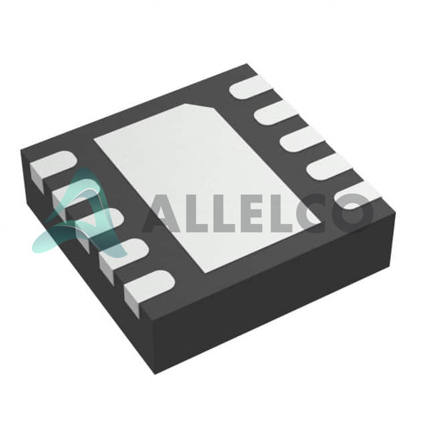
Compact 10-VSON package with exposed thermal pad
Flexible implementation with adjustable output voltage and switching frequency
Robust thermal management and overcurrent protection
Key Technical Parameters
Output Voltage: 0.8V to 24V
Output Current: Up to 3A
Switching Frequency: 50kHz to 1.5MHz
Input Voltage: 4.5V to 28V
Operating Temperature: -40°C to 150°C

TPS54335ADRCR (4)
Quality and Safety Features
ROHS3 compliant
Thermal shutdown and overcurrent protection
Compatibility
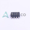
Surface mount package, suitable for a variety of PCB designs

TPS54335ADRCR (5)
Application Areas
Suitable for a wide range of applications, including industrial, automotive, and consumer electronics
Product Lifecycle
This product is currently in active production and not nearing discontinuation.
Replacement or upgraded models may become available in the future.
Key Reasons to Choose This Product
High-performance and efficient step-down DC-DC conversion
Flexible configuration options for customized power solutions
Robust thermal and overcurrent protection for reliable operation
Compact package size and surface mount design for space-constrained applications
Proven reliability and quality from a trusted manufacturer, Texas Instruments


 TPS54336ADDARTexas InstrumentsIC REG BUCK ADJUSTABLE 3A 8SOPWR
 TPS54335ADDATexas InstrumentsIC REG BUCK ADJUSTABLE 3A 8SOPWR
 TPS54335ADDARTexas InstrumentsIC REG BUCK ADJUSTABLE 3A 8SOPWR
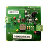 TPS54335AEVM-010Texas InstrumentsEVAL BOARD FOR TPS54335A
 TPS54336ADDATexas InstrumentsIC REG BUCK ADJUSTABLE 3A 8SOPWR
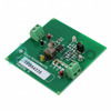 TPS54335EVM-556Texas InstrumentsEVALUATION BOARD FOR TPS54335
 TPS54335ATexas Instruments


