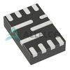

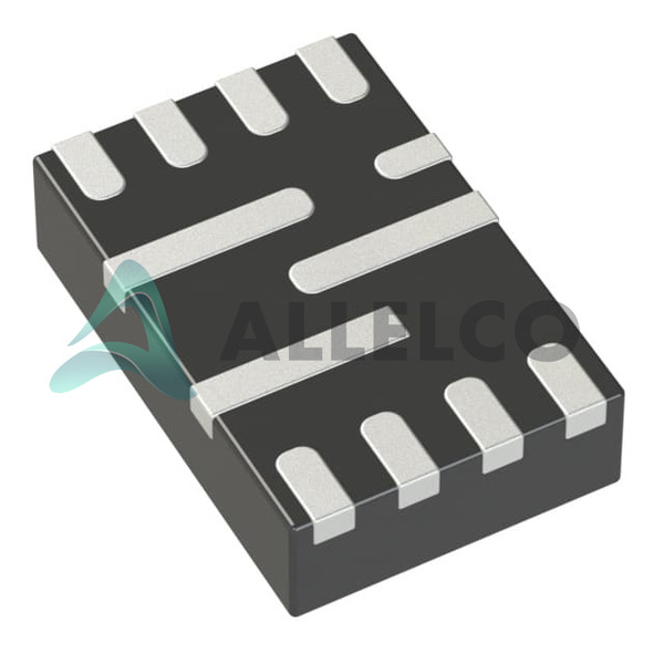
TPS566235RJNR (1)
Manufacturer Part Number
TPS566235RJNR
Manufacturer
Texas Instruments
Introduction
High-efficiency step-down voltage regulator from Texas Instruments' Eco-Mode™ series for power management.
Product Features and Performance
Eco-Mode™ series for enhanced power conservation
Step-Down functionality for voltage reduction
Positive output configuration
Buck topology for efficient conversion
Adjustable output for versatile applications
Single output design
Input voltage range from 4.5V to 18V
Adjustable output voltage from 0.6V to 7V
Capable of delivering up to 6A of output current
600kHz switching frequency for a good balance between efficiency and component size
Built-in synchronous rectifier for improved efficiency
Surface mount design for modern PCB layout
Product Advantages
High efficiency and low power consumption in Eco-Mode™
Wide input voltage range compatible with various power sources
Flexibility with adjustable output voltage
High current output suitable for demanding applications
Fast switching frequency allowing a smaller size of external components
Optimized for thermal performance within a -40°C to 125°C operating range
TPS566235RJNR (2)
Key Technical Parameters
Voltage - Input (Min): 4.5V
Voltage - Input (Max): 18V
Voltage - Output (Min/Fixed): 0.6V
Voltage - Output (Max): 7V
Current - Output: 6A
Frequency - Switching: 600kHz
Quality and Safety Features
Operational temperature range from -40°C to 125°C ensures reliability in various environments
Compatibility
Compatible with a variety of applications requiring an adjustable output voltage
Suitable for surface mounting on a variety of PCBs
Application Areas
Power supply for industrial systems
Consumer electronics
Telecommunications
Computing devices
Networking equipment
Product Lifecycle
Active status, not nearing discontinuation
Availability of replacements or upgrades within Texas Instruments' portfolio
Several Key Reasons to Choose This Product
Efficient power conversion reducing overall energy waste
Wide input voltage accommodating a vast array of power sources
Ability to provide a high output current for high-power applications
Adjustable output facilitating use in multiple applications
High-frequency operation minimizing the size of passive components
Synchronous rectification boosting efficiency
Robust thermal performance expanding the range of operating conditions
Reputable manufacturer with a track record for quality and reliability
Ongoing product support and availability in the market


 TPS566231EVMTexas Instruments3-V TO 17-V VIN, 6-A SYNCHRONOUS
 TPS56528DDARTexas InstrumentsIC REG BUCK ADJUSTABLE 5A 8SOPWR
 TPS566238PEVMTexas InstrumentsTPS566238P 6-A SYNCHRONOUS STEP-
 TPS566238EVMTexas Instruments3-V TO 17-V VIN, 6-A SYNCHRONOUS
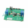 TPS566231PEVMTexas InstrumentsTPS566231P 6-A SYNCHRONOUS STEP-
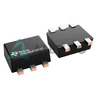 TPS566242DRLRTexas InstrumentsIC REG BUCK ADJ 6A SOT563
 TPS56528EVM-534Texas InstrumentsEVAL MODULE FOR TPS56528
 TPS566235EVM-036Texas InstrumentsPOWER MANAGEMENT
 TPS565P3/TXBelden Inc.3 PC SPLICE CONN, 565 P3/TX
 TPS566242DRLR


