

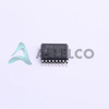
 TPS61030PWPRTexas InstrumentsIC REG BOOST ADJ 3.6A 16HTSSOP
 TPS61032EVM-208Texas InstrumentsEVAL MOD FOR TPS61032
 TPS61030EVM-208Texas InstrumentsEVAL MOD FOR TPS61030
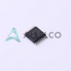 TPS61030PWPTexas InstrumentsIC REG BOOST ADJ 3.6A 16HTSSOP
 TPS61031EVM-208Texas InstrumentsEVAL MOD FOR TPS61031
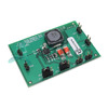 TPS61030EVM-029Texas InstrumentsEVALUATION MODULE FOR TPS61030
 TPS61032PWPTexas InstrumentsIC REG BOOST 5V 3.6A 16HTSSOP
- Nath***rooks
- Jun 11, 2026
HomeProductsIntegrated Circuits (ICs)PMIC - Voltage Regulators - DC DC Switching RegulatorsTPS61030RSARG4
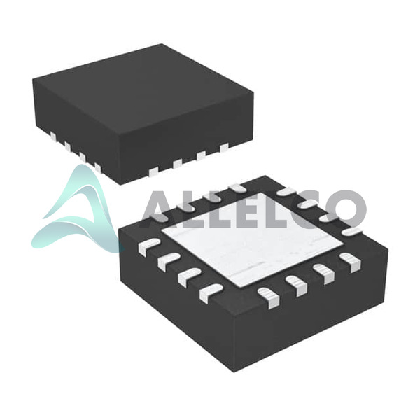

Image may be representation.
See specifications for product details.
See specifications for product details.
- EXPRESS OPTION
- Payment method
TPS61030RSARG4 - Texas Instruments
- Manufacturer Part Number
- TPS61030RSARG4
- Manufacturer
- Texas Instruments
- Allelco Part Number
- 98D-TPS61030RSARG4
- Warranty
- 1 Year Allelco Warranty - Find out more
- Stock Status:
- 10,948 pcs available, New & Original
- Parts Description
- IC REG BOOST ADJ 3.6A 16QFN
- Package
- 16-QFN (4x4)
- Data sheet
-
TPS61030RSARG4.pdf
HTML Datasheet
TPS61030-32.pdf
- RoHs Status
- ROHS3 Compliant
- Our certification
- In stock: 10948


