
TPS61061YZFT (1)
Manufacturer Part Number
TPS61061YZFT
Manufacturer
Texas Instruments
Introduction
The TPS61061YZFT is a step-up (boost) DC-DC regulator LED driver, designed for powering backlight applications. It features an integrated switch and supports PWM dimming.
Product Features and Performance
Type: DC DC Regulator
Topology: Step-Up (Boost)
Internal Switch(s): Yes
Number of Outputs: 1
Voltage Supply (Min): 2.7V
Voltage Supply (Max): 6V
Voltage Output: 18.5V
Current Output / Channel: 400mA (Switch)
Frequency: 1MHz
Dimming: PWM
Operating Temperature: -40°C ~ 85°C (TA)
Mounting Type: Surface Mount
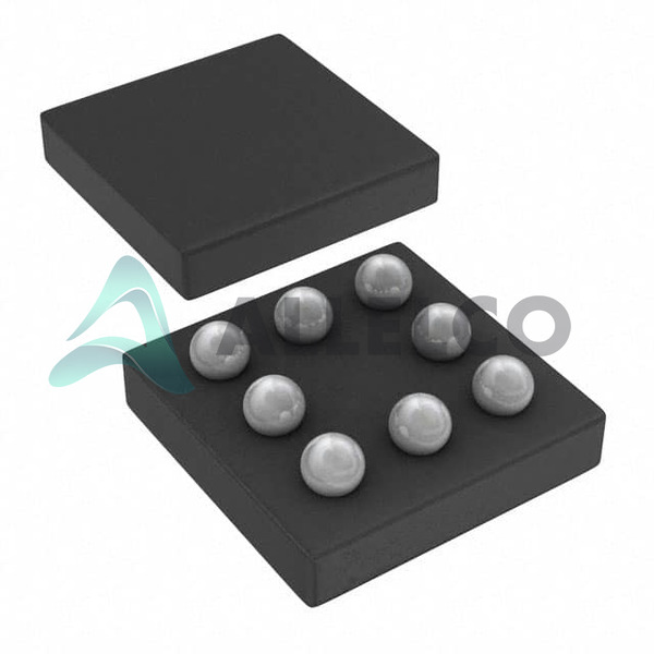
Package / Case: 8-UFBGA, DSBGA
Supplier Device Package: 8-DSBGA
Product Advantages
High output voltage of 18.5V suitable for driving LEDs in series.
Wide input voltage range of 2.7V to 6V allowing for various battery configurations.
Integrated power switch to save space and reduce external component count.
High frequency operation (1MHz) enabling the use of smaller, low-cost external components.
PWM dimming capability provides flexible brightness control.
Key Technical Parameters
Input Voltage: 2.7V to 6V
Output Voltage: 18.5V
Output Current: 400mA
Switching Frequency: 1MHz
Operating Temperature Range: -40°C to 85°C
Quality and Safety Features
Over-temperature protection
Over-current protection
Built-in thermal shutdown
Compatibility
Compatible with a wide range of LED configurations due to its adjustable output voltage.
Application Areas
LED Backlighting for displays
Portable and battery-powered devices requiring high brightness LED drivers
Product Lifecycle
Product Status: Active
Not nearing discontinuation, with ongoing manufacturer support and availability of parts.
Several Key Reasons to Choose This Product
Efficient power conversion for maximized battery life.
Compact 8-DSBGA package ideal for space-constrained applications.
High level of integration reduces complexity and potential points of failure.
Reliable operation under a wide range of environmental conditions.
Support for advanced dimming techniques enhances user experience in display applications.
 TPS61070DDCRTexas InstrumentsIC REG BOOST ADJ 500MA TSOT23-6
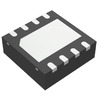 TPS61061DRBRG4Texas InstrumentsIC LED DRVR RGLTR PWM 400MA 8SON
 TPS61070DDCRG4Texas InstrumentsIC REG BOOST ADJ 500MA TSOT23-6
 TPS61061EVM-091Texas InstrumentsEVALUATION MOD FOR TPS61061-091
 TPS61062YZFTexas Instruments


