

TPS61090RSAR (1)
Manufacturer Part Number
TPS61090RSAR
Manufacturer
Texas Instruments
Introduction
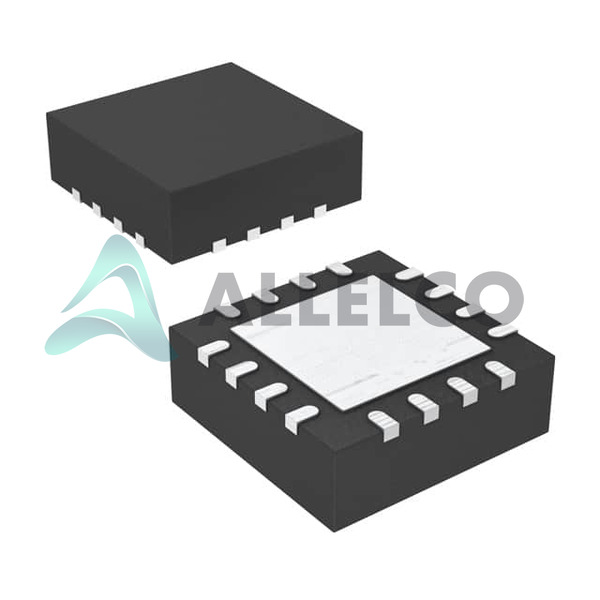
The TPS61090RSAR is a high-efficiency step-up DC-DC converter in Texas Instruments' power management portfolio.
Product Features and Performance
Step-Up (Boost) regulator
Output configuration is positive
Adjustable output type
Features a synchronous rectifier for improved efficiency
Supports a frequency of switching at 600kHz
Operates with a single output
Designed for surface mount technology
Product Advantages
High efficiency due to synchronous rectification
Wide input voltage range suitable for multiple applications
Adjustable output voltage for flexible use
Up to 2A switch current output for high-power applications
Capable of operating across a wide temperature range

TPS61090RSAR (2)
Key Technical Parameters
Voltage - Input (Min): 1.8V
Voltage - Input (Max): 5.5V
Voltage - Output (Min/Fixed): 1.8V
Voltage - Output (Max): 5.5V
Current - Output: 2A (Switch)
Frequency - Switching: 600kHz
Temperature Range: -40°C ~ 85°C (TA)
Quality and Safety Features
Built to operate reliably over a wide temperature range of -40°C to 85°C
Compatibility
Suitable for a variety of applications requiring voltage boost functionality
Compatible with other components that require an adjustable boost voltage regulator
Compatible with surface mount technology fabrication
Application Areas
Suitable for portable electronics, battery-powered devices, and power backup systems
Ideal for IoT devices and smart sensors
Useful in consumer electronics that require power boosting from batteries
Product Lifecycle
Product Status: Active
Continued manufacturer support and no imminent discontinuation
Several Key Reasons to Choose This Product
Efficient power conversion resulting in extended battery life
Flexible application due to a wide input and output voltage range
Capability to drive loads up to 2A, suitable for high-power demands
Compact 16-VQFN Exposed Pad package saves board space
Components from Texas Instruments are renowned for their reliability and performance
On-going manufacturer support ensures long-term usability and updates
Advanced thermal design of the package allows operation in various environments


 TPS61088RHLRTexas InstrumentsIC REG BOOST ADJ 10A 20VQFN
 TPS61093DSKRTexas InstrumentsIC REG BOOST ADJ 900MA 10SON
 TPS61093EVM-519Texas InstrumentsEVAL MODULE FOR TPS61093-519
 TPS61089RNRTTexas InstrumentsIC REG BOOST ADJ 7A 11VQFN
 TPS61089RNRRTexas InstrumentsIC REG BOOST ADJ 7A 11VQFN
 TPS61090EVM-029Texas InstrumentsEVAL MODULE FOR TPS61090-029
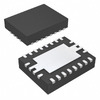 TPS61088RHLTTexas InstrumentsIC REG BOOST ADJ 10A 20VQFN
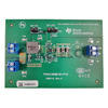 TPS61089EVM-742Texas InstrumentsEVALUATION MODULE
 TPS61093DSKTTexas InstrumentsIC REG BOOST ADJ 900MA 10SON


