View All

Please refer to the English Version as our Official Version.Return

Europe
France(Français) Germany(Deutsch) Italy(Italia) Russian(русский) Poland(polski) Czech(Čeština) Luxembourg(Lëtzebuergesch) Netherlands(Nederland) Iceland(íslenska) Hungarian(Magyarország) Spain(español) Portugal(Português) Turkey(Türk dili) Bulgaria(Български език) Ukraine(Україна) Greece(Ελλάδα) Israel(עִבְרִית) Sweden(Svenska) Finland(Svenska) Finland(Suomi) Romania(românesc) Moldova(românesc) Slovakia(Slovenská) Denmark(Dansk) Slovenia(Slovenija) Slovenia(Hrvatska) Croatia(Hrvatska) Serbia(Hrvatska) Montenegro(Hrvatska) Bosnia and Herzegovina(Hrvatska) Lithuania(lietuvių) Spain(Português) Switzerland(Deutsch) United Kingdom(English)
Asia/Pacific
Japan(日本語) Korea(한국의) Thailand(ภาษาไทย) Malaysia(Melayu) Singapore(Melayu) Vietnam(Tiếng Việt) Philippines(Pilipino)
Africa, India and Middle East
United Arab Emirates(العربية) Iran(فارسی) Tajikistan(فارسی) India(हिंदी) Madagascar(malaɡasʲ)
South America / Oceania
New Zealand(Maori) Brazil(Português) Angola(Português) Mozambique(Português)
North America
United States(English) Canada(English) Haiti(Ayiti) Mexico(español)
HomeProductsIntegrated Circuits (ICs)PMIC - Voltage Regulators - DC DC Switching RegulatorsTPS62110RSAR
TPS62110RSAR Image
Image may be representation.
See specifications for product details.
EXPRESS OPTION
Payment method

TPS62110RSAR - Texas Instruments

Manufacturer Part Number
TPS62110RSAR
Manufacturer
Texas Instruments
Allelco Part Number
32D-TPS62110RSAR
Warranty
1 Year Allelco Warranty - Find out more
Stock Status:
39,255 pcs available, New & Original
Parts Description
IC REG BUCK ADJ 1.5A 16QFN
Package
16-QFN (4x4)
Data sheet
TPS62110RSAR.pdf

PCN Design/Specification

Mult Dev Material Chg 29/Mar/2018.pdf

HTML Datasheet

TPS62110-13.pdf
RoHs Status
ROHS3 Compliant
Our certification
In stock: 39255
  • Unit Price: $0.423
  • Subtotal: $0.00

Want a better price?
Add to Cart and Submit RFQ now, we'll contact you immediately.

Quantity Unit Price Ext. Price
1+ $0.423 $0.42
10+ $0.344 $3.44
30+ $0.304 $9.12
100+ $0.266 $26.60
500+ $0.243 $121.50
1000+ $0.23 $230.00
The above prices does not include taxes and freight rates, which will be calculated on the order pages.

Specifications

TPS62110RSAR Tech Specifications
Texas Instruments - TPS62110RSAR technical specifications, attributes, parameters and parts with similar specifications to Texas Instruments - TPS62110RSAR

Product Attribute Attribute Value
Manufacturer Texas Instruments
Voltage - Output (Min/Fixed) 1.2V
Voltage - Output (Max) 16V
Voltage - Input (Min) 3.1V
Voltage - Input (Max) 17V
Topology Buck
Synchronous Rectifier Yes
Supplier Device Package 16-QFN (4x4)
Series -
Package / Case 16-VQFN Exposed Pad
Product Attribute Attribute Value
Package Tape & Reel (TR)
Output Type Adjustable
Output Configuration Positive
Operating Temperature -40°C ~ 125°C (TJ)
Number of Outputs 1
Mounting Type Surface Mount
Function Step-Down
Frequency - Switching 1MHz
Current - Output 1.5A
Base Product Number TPS62110

Environmental & Export Classifications

ATTRIBUTE DESCRIPTION
RoHs Status ROHS3 Compliant
Moisture Sensitivity Level (MSL) 2 (1 Year)
REACH Status REACH Unaffected
ECCN EAR99
HTSUS 8542.39.0001

Parts Introduction

TPS62110RSAR Image
TPS62110RSAR (1)

Manufacturer Part Number

TPS62110RSAR

Manufacturer

Texas Instruments

Introduction

The TPS62110RSAR is a highly efficient, synchronous step-down DC/DC converter from Texas Instruments, designed for use in power management applications.

Product Features and Performance

Step-down (Buck) topology

Adjustable output type

Capable of driving 1.5A output current

Wide input voltage range from 3.1V to 17V

Output voltage adjustable from 1.2V to 16V

High switching frequency of 1MHz

Synchronous rectifier integrated for improved efficiency

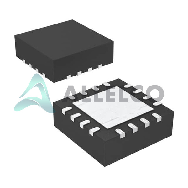
Designed for surface mount technology with a 16-VQFN exposed pad package

Operating temperature range from -40°C to 125°C

Product Advantages

High efficiency and power density

Flexibility in input and output voltage selection

Suitable for battery-powered devices due to low minimum input voltage

Thermal and over-current protections improve product reliability

TPS62110RSAR Image
TPS62110RSAR (2)

Key Technical Parameters

Voltage Input (Min): 3.1V

Voltage Input (Max): 17V

Voltage Output (Min/Fixed): 1.2V

Voltage Output (Max): 16V

Current Output: 1.5A

Frequency Switching: 1MHz

Operating Temperature: -40°C ~ 125°C (TJ)

Quality and Safety Features

Over-current protection

Thermal shutdown

Wide operating temperature range ensuring stability across various environments

Compatibility

Compatible with a range of devices requiring adjustable voltage and high power efficiency

Suitable for a multitude of electronic devices across different sectors due to versatile input and output specifications

Application Areas

Consumer Electronics

Telecommunications Equipment

Portable Devices

Power Supply Units

Product Lifecycle

Current Status: Active

Not nearing discontinuation; replacements and upgrades available

Several Key Reasons to Choose This Product

High efficiency, minimizing heat generation and maximizing battery life

Flexibility offered through wide input and output voltage range

High reliability and safety features protecting against potential damage

Compact and lightweight design suitable for modern, space-constrained applications

High-frequency operation resulting in smaller external components

Frequently Asked Questions(FAQ)

How does the TPS62110RSAR handle thermal performance under continuous 1.5A load conditions in a compact 4x4mm QFN package, and what design considerations are necessary to ensure reliable operation near its maximum junction temperature?
The TPS62110RSAR integrates advanced power management features that support high-efficiency step-down conversion in space-constrained applications. With an internal synchronous rectifier and 1MHz switching frequency, it achieves typical efficiency exceeding 90% at moderate loads, reducing conduction and switching losses. However, under sustained 1.5A output current, power dissipation increases significantly—especially when input-to-output differential voltage is large. For example, at Vin = 5V and Vout = 3.3V, power loss approximates (5 - 3.3) × 1.5A = 2.55W. In a 16-QFN (4x4) package with exposed pad, this necessitates effective PCB thermal management: mounting the exposed pad to a solid copper plane and using multiple thermal vias to inner ground layers helps dissipate heat. Without adequate heatsinking, junction temperatures may approach or exceed 125°C, potentially triggering thermal shutdown. Therefore, thermal simulation and layout optimization are essential for long-term reliability in compact designs.
What are the key differences between the TPS62110RSAR and other buck regulators in Texas Instruments’ portfolio like the TPS62260 or TPS62840, particularly regarding efficiency, footprint, and minimum input voltage requirements?
The TPS62110RSAR targets medium-current applications requiring adjustable output voltages and wide input flexibility up to 17V, making it suitable for industrial and automotive systems. Compared to the TPS62260—a 1A device with fixed 3.3V/5V outputs—the TPS62110RSAR offers greater design flexibility through adjustable output but trades peak efficiency slightly due to larger die size and higher gate drive currents. The TPS62840, designed for ultra-low quiescent current (as low as 1.5µA), sacrifices switching frequency (typically 2.25MHz) and maximum output current (1A) for battery life optimization. Unlike both, the TPS62110RSAR maintains 1.5A capability and 1MHz operation, balancing efficiency with power density. Its adjustable output range (1.2V–16V) also enables compatibility with post-LDO architectures where tighter noise margins are required. Thus, selection hinges on whether adjustable voltage, higher current, or ultralow standby power takes precedence.
Can the TPS62110RSAR be used safely in automotive environments, and how do its specifications support functional safety considerations?
While the TPS62110RSAR operates across a commercial temperature range (-40°C to +125°C TJ), its qualification level does not inherently meet AEC-Q100 Grade 1 unless explicitly stated by the manufacturer. It can be deployed in non-critical automotive subsystems such as infotainment or body electronics if design-in practices include robust EMC filtering, transient protection, and derating of electrical parameters. The device’s 17V maximum input withstands load dump transients common in automotive applications better than lower-voltage regulators. Additionally, its integrated soft-start prevents inrush surges during hot-plug events. However, for ASIL-rated functions, a functionally qualified automotive-grade variant (e.g., from TI’s AEC-Q100 compliant family) should be selected instead. Designers must verify compliance with relevant standards based on application context.
What layout guidelines are critical when implementing the TPS62110RSAR to minimize electromagnetic interference (EMI) and maintain stable operation at 1MHz switching frequency?
Minimizing parasitic inductance in the high-current loop formed by the inductor, input capacitor, and SW pin is paramount for the TPS62110RSAR. Place ceramic input capacitors (preferably X7R or X5R) as close as possible to the VIN and GND pins, with short, wide traces connecting them directly to the IC. The feedback divider resistors should be located near the FB pin to avoid noise pickup on the sensitive feedback node. Keep the SW node area small and avoid routing sensitive signals underneath it. Use a continuous ground plane beneath the IC and connect the exposed pad via multiple vias to ensure low-impedance return paths. Proper decoupling of the COMP pin with a small capacitor (typically 10nF) enhances stability under fast load transients. These measures help suppress conducted emissions and maintain phase margin across temperature and load variations.
How does the adjustable output voltage range of the TPS62110RSAR influence system-level design trade-offs in terms of inductor selection, efficiency, and transient response?
The TPS62110RSAR’s adjustable output (1.2V to 16V) allows tailoring the converter to precise load requirements, which directly affects component selection. For low Vout (e.g., 1.2V), smaller inductors can be used due to higher ripple current relative to average current, improving transient response but increasing ripple voltage. Conversely, at higher Vout (e.g., 12V), inductor values typically increase to limit ripple current, which improves efficiency but slows down load-step recovery. Efficiency also varies: peak efficiency often occurs near mid-range ratios (e.g., Vin = 5V, Vout = 3.3V), so operating at extreme ratios may reduce overall system efficiency. Designers must balance these factors by selecting inductors with appropriate saturation current (>1.8A for headroom) and DCR, while ensuring the control loop remains stable across the entire adjustment range—especially important when using external compensation networks.
Is it feasible to parallel two TPS62110RSAR devices to increase total output current beyond 1.5A, and what challenges arise in doing so?
Parallel operation of the TPS62110RSAR is not recommended without significant modifications. The devices lack inherent current sharing mechanisms, leading to unequal distribution due to manufacturing tolerances in threshold voltages and duty cycles. One unit may carry most of the current, risking overheating and premature failure. Achieving balanced sharing would require external circuitry such as sense resistors and active control loops, adding complexity and cost. Moreover, the 1MHz switching frequency creates beat frequencies that complicate EMI filtering and could interfere with nearby RF components. Instead, designers are advised to select a single regulator capable of meeting the full current requirement—such as the TPS63020 or higher-current TI buck regulators—or use a discrete multiphase solution if scalability is essential.
What impact does the 1MHz switching frequency have on component selection for the TPS62110RSAR, particularly regarding inductor size, EMI characteristics, and filter design?
The TPS62110RSAR’s 1MHz switching frequency enables the use of smaller magnetics compared to lower-frequency converters, reducing board space and improving dynamic response. Inductors with lower inductance values (e.g., 2.2µH instead of 4.7µH) can be employed while maintaining acceptable ripple current. This benefits portable and space-limited applications. However, higher switching frequency increases high-frequency conducted and radiated emissions, necessitating careful PCB layout and shielding. Output filters require capacitors with low ESR and sufficient ripple current rating; ceramic capacitors dominate due to their low profile and stability. Careful attention to trace lengths and grounding minimizes conducted noise into adjacent circuits. Additionally, the 1MHz operation places harmonics within CISPR 25 Class 5 limits only if properly managed, making this topology suitable for consumer electronics but requiring extra scrutiny in sensitive RF environments.
How does the TPS62110RSAR perform in terms of startup behavior and inrush current limitation, especially when powered from a capacitive load or battery source?
The TPS62110RSAR features soft-start functionality controlled internally, typically ramping up in approximately 1ms to limit inrush current during startup. This protects both the input supply and downstream components from voltage droop or brownouts. When connected to a battery, the soft-start ensures gradual energy delivery, extending battery life by avoiding sudden high-current draws. Under capacitive loads (e.g., >100µF), the ramp time remains consistent due to internal current limiting, though very large capacitances may extend the soft-start duration slightly. The device also includes undervoltage lockout (UVLO) to prevent unintended operation near dropout. Designers should ensure that the soft-start time aligns with system initialization sequences, particularly in microcontrollers that expect regulated rails before asserting reset signals.
Can the TPS62110RSAR operate reliably with input voltages above 12V, and what precautions should be taken to manage stress on internal components?
Yes, the TPS62110RSAR supports input voltages up to 17V, making it suitable for applications involving unregulated wall adapters or batteries with voltage spikes. At high input voltages (e.g., 15V or 17V), the duty cycle drops significantly even at moderate output levels (e.g., 3.3V), increasing conduction losses in the high-side MOSFET. More critically, the internal gate drivers experience higher stress due to increased Miller plateau effects, potentially affecting switching transitions and efficiency. To mitigate this, ensure that the input capacitor has sufficient voltage rating (at least 25V for robustness) and that the PCB traces handle peak currents without excessive IR drop. Thermal monitoring becomes increasingly important, and layout should prioritize minimizing parasitic resistance in the power path to avoid localized heating.
What role does the internal compensation network play in the TPS62110RSAR, and when might external compensation be necessary?
The TPS62110RSAR uses a fixed internal compensation network optimized for standard inductor values (typically 2.2µH to 4.7µH) and typical output capacitance ranges (ceramic-based). This simplifies design and ensures stability across most common configurations. However, under certain conditions—such as very low ESR output capacitors (e.g., single ceramic cap <10µF), large output capacitance (>22µF), or extreme load steps—the phase margin may degrade, leading to ringing or instability. In such cases, external compensation using a resistor-capacitor network at the COMP pin can improve transient response and stability. Designers should consult the datasheet’s stability graphs and test prototypes under worst-case load transients to determine if modification is needed. External compensation is rarely required but provides flexibility for fine-tuning performance.
How does the TPS62110RSAR support power sequencing or enable/disable functions in multi-rail systems?
The TPS62110RSAR lacks a dedicated EN pin but relies on the VIN rail for enabling. Power-up occurs when VIN exceeds the UVLO threshold (~3.1V minimum), and power-down happens gradually upon VIN falling below UVLO. This makes it challenging to implement precise sequencing with respect to other rails lacking EN control. However, some applications leverage the open-drain PG (power good) output (if available in specific variants) to signal regulation status. If sequencing is critical, designers may add an external enable circuit using a supervisor IC or microcontroller GPIO to hold the EN pin (if present in alternative packages) or use a separate LDO with sequencing capabilities. Alternatively, cascading regulators with built-in sequencing can achieve desired turn-on/off timing across multiple supplies.
What are the implications of operating the TPS62110RSAR near its minimum input voltage (3.1V) with an output close to 1.2V, and how does dropout behave in this region?
Near the minimum input voltage of 3.1V and minimum output of 1.2V, the TPS62110RSAR operates at nearly unity duty cycle, approaching its dropout limit. In practice, dropout voltage is typically 100–300mV depending on load and process variation, meaning the input must remain at least 1.3V–1.5V above the output to regulate effectively. At 3.1V input and 1.2V output, the device may struggle to maintain regulation under full load, resulting in droop or complete loss of output voltage. This condition increases conduction losses in the high-side switch and reduces efficiency. Designers should maintain a reasonable margin (e.g., ≥0.5V) between VIN and VOUT to ensure reliable operation, especially in battery-powered systems where discharge curves bring voltages down over time.
How does the TPS62110RSAR compare to linear regulators in terms of efficiency, thermal dissipation, and suitability for stepping down high-voltage sources?
The TPS62110RSAR significantly outperforms linear regulators (LDOs) in efficiency and thermal handling when stepping down high voltages. For instance, converting 12V to 3.3V at 1A yields ~77% efficiency in a buck configuration versus ~28% in a linear regulator—reducing power loss from 8.7W to 2.3W. This translates to much lower junction temperatures and eliminates the need for bulky heatsinks. Even at light loads, the TPS62110RSAR maintains >85% efficiency thanks to synchronous rectification and low quiescent current (typically <20µA). Linear regulators cannot efficiently handle large differential voltages without excessive dissipation, making the TPS62110RSAR ideal for post-buck applications where further regulation is needed, but only after initial conversion to a lower intermediate voltage.
Are there any known limitations or caveats when using the TPS62110RSAR with ferrite-core inductors versus powdered-iron types, and how do they affect performance?
The TPS62110RSAR performs well with both ferrite and powdered-iron core inductors, but material choice impacts efficiency, size, and cost. Ferrite cores offer higher permeability and lower core losses at 1MHz, supporting smaller footprints and better efficiency—ideal for compact designs. Powdered-iron cores tolerate saturation better under high ripple current but exhibit higher hysteresis losses, reducing efficiency and increasing heat generation. For the TPS62110RSAR’s 1.5A output, selecting an inductor with a saturation current rating above 2A (e.g., 2.2µH, 2.5A sat) ensures headroom. Designers should verify that core losses remain within acceptable limits at peak switching frequency and load, as excessive losses can elevate IC temperature and compromise long-term reliability.

Parts with Similar Specifications

The three parts on the right have similar specifications to Texas Instruments TPS62110RSAR

Product Attribute TPS62110QRSARQ1 TPS62110QRSAREP TPS62110MRSAREP TPS62111RSAR
Part Number TPS62110QRSARQ1 TPS62110QRSAREP TPS62110MRSAREP TPS62111RSAR
Manufacturer Texas Instruments Texas Instruments Texas Instruments Texas Instruments
Voltage - Output (Min/Fixed) - - - -
Package - Tape & Reel (TR) Tube Tape & Reel (TR)
Operating Temperature - -40°C ~ 85°C 0°C ~ 70°C -40°C ~ 85°C
Series - - - -
Function - - - -
Supplier Device Package - 196-NFBGA (12x12) 16-PDIP 64-VQFN (9x9)
Mounting Type - Surface Mount Through Hole Surface Mount
Voltage - Input (Min) - - - -
Package / Case - 196-LFBGA 16-DIP (0.300', 7.62mm) 64-VFQFN Exposed Pad
Voltage - Output (Max) - - - -
Voltage - Input (Max) - - - -
Synchronous Rectifier - - - -
Current - Output - - - -
Topology - - - -
Output Configuration - - - -
Number of Outputs - - - -
Base Product Number - DAC34H84 MAX500 ADS62P42
Output Type - Current - Unbuffered Voltage - Buffered -
Frequency - Switching - - - -

TPS62110RSAR Datasheet PDF

Download TPS62110RSAR pdf datasheets and Texas Instruments documentation for TPS62110RSAR - Texas Instruments.

PCN Design/Specification
Mult Dev Material Chg 29/Mar/2018.pdf
HTML Datasheet
TPS62110-13.pdf

Customer Reviews

Evaluation: 10 Articles

  • Nath***rooks
    Jun 11, 2026

    Installed this power component in a converter board. Output remained stable under different load conditions and thermal performance was better than expected.

  • Dani***alkerTech
    Jun 1, 2026

    Product works, but setup took more effort than expected. Once configured the MCU ran reliably, although documentation support felt older compared with newer platforms. Fine for maintenance projects.

  • Yuki***aka88
    May 26, 2026

    信号通信プロジェクトでこのRS-485トランシーバーを使用しました。設置は簡単で、長距離ケーブルでも通信は安定していました。消費電力も、以前使用していたものより低くなっています。

  • Stev***aker
    May 20, 2026

    Solid diode for power rectification. Works well in switching circuits.

  • Bran***Lewis
    May 11, 2026

    Compact FPGA with good performance. Suitable for basic signal processing tasks.

  • Oliv***arris
    May 7, 2026

    Reliable I/O expander. Works well in embedded control applications.

  • Jess***Jones
    Apr 17, 2026

    It offers good value for the price, and the specifications match the description. I’ve been using it for two days with no issues, and I’ll definitely buy it again if I need it in the future.

  • Mich***Smith
    Apr 17, 2026

    Shipping was on time, the component pins are neatly aligned, and I tested 10 of them with a multimeter—all readings were within the specified range. Highly recommended.

  • Aman***arris
    Apr 3, 2026

    It was great—the entire process, from placing the order to receiving the package, went very smoothly. The components were consistent, the price was fair, and I had a very pleasant shopping experience.

  • Mike***nch
    Apr 3, 2026

    Better than expected! The resistance and capacitance readings were spot-on, and it passed the test on the first try. The service was reliable, and the packaging was thoughtful—I highly recommend it.

Write a Review

Your Email address will not be published.

Shipment

Delivery Time

In-stock items can be shipped within 24 hours. Some parts will be arranged for delivery within 1-2 days from the date all items arrive at our warehouse. And Allelco ships order once a day at about 17:00, except Sunday. Once the goods are shipped, the estimated delivery time depends on the shipping methods and Delivery destination. The table below shows are the logistic time for some common countries.

Delivery Cost

  1. Use your express account for shipment if you have one.
  2. Use our account for the shipment. Refer to the table below for the approximate charges.
(Different time frame / countries / package size has different price.)

Delivery Method

  1. Global Common Shipment by DHL / UPS / FedEx / TNT / EMS / SF we support.
  2. Others more shipping ways, please get in touch with your customer manager.

Common Countries Logistic Time Reference
Region Country Logistic Time(Day)
America United States 5
Brazil 7
Europe Germany 5
United Kingdom 4
Italy 5
Oceania Australia 6
New Zealand 5
Asia India 4
Japan 4
Middle East Israel 6
DHL & FedEx Shipment Charges Reference
Shipment charges(KG) Reference DHL(USD$)
0.00kg-1.00kg USD$30.00 - USD$60.00
1.00kg-2.00kg USD$40.00 - USD$80.00
2.00kg-3.00kg USD$50.00 - USD$100.00
Note:
The above table is for reference only. There may have some data bias for the uncontrollable factors.
Contact us if you have any questions.
  • QC (Quality Warranty)
  • Payment Support
  • Packaging
  • Certifications & Memberships

QC (Quality Warranty)

Allelco is committed to exceeding customer expectations through customer service excellence, order accuracy, and on-time delivery.
This is achieved through our commitment to the continual improvement of our processes, services, and products.


Strict quality inspection builds a solid foundation for electronic component quality.
  1. Visual inspection
  2. Performance testing and reliability verification
  3. Standardized full-process testing
  4. Precise control of every parameter
We eliminate defective components and ensure the stable operation of electronic devices through professional quality standards.

Payment Support

The payment method can be chosen from the methods shown below: Wire Transfer (T/T, Bank Transfer), Western Union, Credit card, PayPal.
  • HKBea
  • Paypal
  • MasterCard
  • Western-Union
  • VISA
Stable Delivery, Sincere Partnership — Your Faithful Supply Chain Partner
  • Efficient Supply Management
  • Cost-Saving Procurement
  • Fast Sourcing & Delivery
Contact us if you have any questions.

Packaging

Electrostatic Discharge Protection and Handling

All electrostatic-sensitive components are handled in accordance with electrostatic discharge control procedures. The products are hermetically sealed in anti-static safe packaging to prevent electrostatic damage. Appropriate labeling is also applied for identification and traceability. This ensures product integrity during storage, handling and transportation.


ESD

Certifications & Memberships

Third-party certified, strict quality control. Our certification
  • ISO 9001: 2015
  • ISO 13485: 2016
  • ISO 14001: 2015
  • ISO 28000: 2007
  • ISO 45001: 2018
  • GB/T 27922-2011
  • SMTA
  • IPC
  • ESD
  • PSMA
TPS62110RSAR Image

TPS62110RSAR

Texas Instruments
32D-TPS62110RSAR

Want a better price? Add to Cart and Submit RFQ now, we'll contact you immediately.

0 RFQ
Shopping cart (0 Items)
It is empty.
Compare List (0 Items)
It is empty.
Feedback

Your feedback matters! At Allelco, we value the user experience and strive to improve it constantly.
Please share your comments with us via our feedback form, and we'll respond promptly.
Thank you for choosing Allelco.

Subject
E-mail
Comments
Captcha
Drag or click to upload file
Upload File
types: .xls, .xlsx, .doc, .docx, .jpg, .png and .pdf.
Max file size: 10MB