

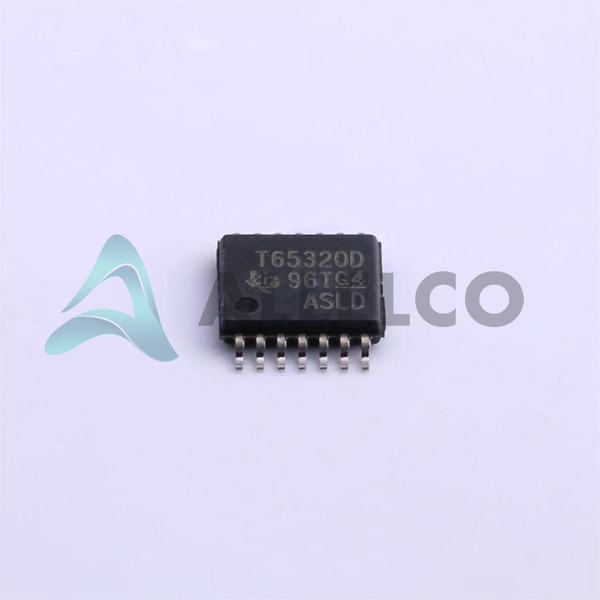
TPS65320DQPWPRQ1 (1)
Manufacturer Part Number
TPS65320DQPWPRQ1
Manufacturer
Texas Instruments
Introduction
Integrated circuit (IC) that provides power management functionality
Product Features and Performance
Dual-channel power management IC (PMIC)
Step-down (buck) converter and linear (LDO) regulator
Switching frequency range of 100 kHz to 2.5 MHz
Supports input voltage range of 3.6 V to 36 V
Output 1: 1.1 V to 20 V, 3.2 A
Output 2: 1.1 V to 5.5 V, 280 mA
Includes voltage supervisor function
Product Advantages
Integrates multiple power management functions in a single chip
Wide input voltage and output voltage ranges
High efficiency power conversion
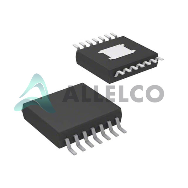
Compact 14-pin HTSSOP package
TPS65320DQPWPRQ1 (2)
Key Technical Parameters
Package: 14-HTSSOP
Mounting type: Surface mount
Operating temperature range: -40°C to 125°C
RoHS compliance: ROHS3 Compliant
Quality and Safety Features
Automotive-qualified, AEC-Q100 certified
Includes safety and protection features
Compatibility
Suitable for a wide range of electronic applications
Application Areas
Automotive electronics
Industrial equipment
Consumer electronics
Product Lifecycle
Currently an active product
No information on discontinuation or availability of replacements/upgrades
Key Reasons to Choose This Product
Integrated dual-channel power management in a compact package
Wide input and output voltage ranges for flexibility
High efficiency and switching frequency for power optimization
Automotive-grade quality and safety features
Suitable for a variety of electronic applications
 TPS65320C-EVMTexas InstrumentsEVALUATION MODULE
 TPS65320EVMTexas InstrumentsEVALUATION BOARD FOR TPS65320
 TPS65321EVMTexas InstrumentsEVALUATION MODULE
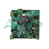 TPS65301EVMTexas InstrumentsEVAL MODULE FOR TPS65301
 TPS65381AQDAPTQ1Texas InstrumentsIC REG AUTOMOTIVE 5OUT 32HTSSOP
 TPS65381EVMTexas InstrumentsEVAL MODULE FOR TPS65381
 TPS65311QRVJRQ1Texas InstrumentsIC PWR MGMT UNIT AUTO 56VQFN
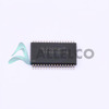 TPS65381AQDAPRQ1Texas InstrumentsIC REG AUTOMOTIVE 5OUT 32HTSSOP
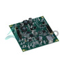 TPS65310AEVMTexas InstrumentsEVAL BOARD FOR TPS65310
 TPS65310AQRVJRQ1Texas InstrumentsIC REG 5OUT BUCK/BST/LNR 56VQFN
 TPS65310QRVJRQ1Texas Instruments


