

TPS65400QRGZRQ1 (1)
Manufacturer Part Number
TPS65400QRGZRQ1
Manufacturer
Texas Instruments
Introduction
Automotive-Grade Step-Down Voltage Regulator with Four Outputs
Product Features and Performance
Step-Down (Buck) Topology
Four Adjustable Outputs
Synchronous Rectifier for Efficiency
Frequency Switching Range: 275kHz to 2.2MHz
Wide Input Voltage Range: 4.5V to 18V
Adjustable Output Voltage: 0.6V to 16.2V
Output Current Capability: 4A and 2A
Supports PWM, Auto and 100% modes
Product Advantages
High-Efficiency Operation
Reduced External Components
Flexible Power Sequencing
Thermal Shutdown Protection
Multiple Output Voltage Configurations
Adjustable Switching Frequency for EMI Management
Key Technical Parameters
Voltage - Input (Min): 4.5V
Voltage - Input (Max): 18V
Voltage - Output (Min/Fixed): 0.6V
Voltage - Output (Max): 16.2V
Current - Output: 4A, 2A
Operating Temperature: -40°C to 125°C (TJ)
Quality and Safety Features
Automotive Grade (AEC-Q100 Qualified)
Over-Temperature Protection
Over-current Protection
Under-voltage Lockout
Compatibility
Surface Mount
Compatible with 48-VFQFN Exposed Pad Package
Application Areas
Automotive Applications
Power Management for Car Infotainment Systems
Advanced Driver-Assistance Systems (ADAS)
Product Lifecycle
Status: Active
No Current Indication of Discontinuation
Replacements and Upgrades Not Specified
Several Key Reasons to Choose This Product
Optimized for Automotive Applications with AEC-Q100 Qualification
Highly Flexible with Four Adjustable Outputs for Comprehensive Power Solutions
Increased System Efficiency and Performance Due to Synchronous Rectification
Durability and Reliability in Harsh Automotive Environments
Optimizable Frequency Switching for Reduced EMI
Easy to Integrate with Standard Surface Mount Technology


 TPS65381AQDAPTQ1Texas InstrumentsIC REG AUTOMOTIVE 5OUT 32HTSSOP
 TPS65510RGTRTexas InstrumentsIC BATT PWR MGMT BACKUP 16QFN
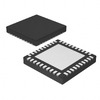 TPS65471RHARTexas InstrumentsIC BATT CHG LI-ION 40VQFN
 TPS65381EVMTexas InstrumentsEVAL MODULE FOR TPS65381
 TPS65400EVM-678Texas InstrumentsIC REG BUCK SYNC ADJ QUAD
 TPS65321EVMTexas InstrumentsEVALUATION MODULE
 TPS65321QPWPRQ1Texas InstrumentsIC REG DL BUCK/LINEAR 14HTSSOP
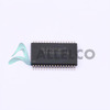 TPS65381AQDAPRQ1Texas InstrumentsIC REG AUTOMOTIVE 5OUT 32HTSSOP
 TPS65520AZVDRTexas InstrumentsIC PWR MGMT FOR DGTL CA 113NFBGA
 TPS653853KPQDCARQ1Texas Instruments


