View All

Please refer to the English Version as our Official Version.Return

Europe
France(Français) Germany(Deutsch) Italy(Italia) Russian(русский) Poland(polski) Czech(Čeština) Luxembourg(Lëtzebuergesch) Netherlands(Nederland) Iceland(íslenska) Hungarian(Magyarország) Spain(español) Portugal(Português) Turkey(Türk dili) Bulgaria(Български език) Ukraine(Україна) Greece(Ελλάδα) Israel(עִבְרִית) Sweden(Svenska) Finland(Svenska) Finland(Suomi) Romania(românesc) Moldova(românesc) Slovakia(Slovenská) Denmark(Dansk) Slovenia(Slovenija) Slovenia(Hrvatska) Croatia(Hrvatska) Serbia(Hrvatska) Montenegro(Hrvatska) Bosnia and Herzegovina(Hrvatska) Lithuania(lietuvių) Spain(Português) Switzerland(Deutsch) United Kingdom(English)
Asia/Pacific
Japan(日本語) Korea(한국의) Thailand(ภาษาไทย) Malaysia(Melayu) Singapore(Melayu) Vietnam(Tiếng Việt) Philippines(Pilipino)
Africa, India and Middle East
United Arab Emirates(العربية) Iran(فارسی) Tajikistan(فارسی) India(हिंदी) Madagascar(malaɡasʲ)
South America / Oceania
New Zealand(Maori) Brazil(Português) Angola(Português) Mozambique(Português)
North America
United States(English) Canada(English) Haiti(Ayiti) Mexico(español)
HomeProductsIntegrated Circuits (ICs)PMIC - Voltage Regulators - LinearTPS7A8012DRBR
TPS7A8012DRBR Image
Image may be representation.
See specifications for product details.
EXPRESS OPTION
Payment method

TPS7A8012DRBR - Texas Instruments

Manufacturer Part Number
TPS7A8012DRBR
Manufacturer
Texas Instruments
Allelco Part Number
32D-TPS7A8012DRBR
Warranty
1 Year Allelco Warranty - Find out more
Stock Status:
39,737 pcs available, New & Original
Parts Description
IC REG LINEAR 1.2V 1A 8SON
Package
8-SON (3x3)
Data sheet
TPS7A8012DRBR.pdf
RoHs Status
ROHS3 Compliant
Our certification
In stock: 39737

Required fields are indicated by an asterisk (*)
Please send RFQ, we will respond immediately.

Quantity

Specifications

TPS7A8012DRBR Tech Specifications
Texas Instruments - TPS7A8012DRBR technical specifications, attributes, parameters and parts with similar specifications to Texas Instruments - TPS7A8012DRBR

Product Attribute Attribute Value
Manufacturer Texas Instruments
Voltage Dropout (Max) 0.5V @ 1A
Voltage - Output (Min/Fixed) 1.2V
Voltage - Output (Max) -
Voltage - Input (Max) 6.5V
Supplier Device Package 8-SON (3x3)
Series -
Protection Features Over Current, Over Temperature, Reverse Polarity, Under Voltage Lockout (UVLO)
Package / Case 8-VDFN Exposed Pad
Package Tape & Reel (TR)
PSRR 48dB ~ 38dB (100Hz ~ 1MHz)
Product Attribute Attribute Value
Output Type Fixed
Output Configuration Positive
Operating Temperature -40°C ~ 125°C (TJ)
Number of Regulators 1
Mounting Type Surface Mount
Current - Supply (Max) 350 µA
Current - Quiescent (Iq) 120 µA
Current - Output 1A
Control Features Enable
Base Product Number TPS7A8012

Environmental & Export Classifications

ATTRIBUTE DESCRIPTION
RoHs Status ROHS3 Compliant
Moisture Sensitivity Level (MSL) 2 (1 Year)
REACH Status REACH Unaffected
ECCN EAR99
HTSUS 8542.39.0001

Parts Introduction

TPS7A8012DRBR Image
TPS7A8012DRBR (1)

Manufacturer Part Number

TPS7A8012DRBR

Manufacturer

Texas Instruments

Introduction

The TPS7A8012DRBR from Texas Instruments is a highly reliable, low drop-out (LDO) linear voltage regulator optimized for power management applications.

Product Features and Performance

Positive output configuration with a fixed output voltage

Low drop-out voltage of up to 0.5V at 1A load

Current output capacity of 1A

Quiescent current of 120 µA

Low supply current of up to 350 µA

Excellent power supply rejection ratio (PSRR) of 48dB to 38dB across 100Hz to 1MHz

Features Enable control for efficient power usage

Equipped with protection features against over current, over temperature, reverse polarity, and under voltage lockout (UVLO)

Product Advantages

High efficiency with lower power dissipation

Extended battery life due to low quiescent current

Robust protection features ensure durability and stability of the application

PSRR enhances noise rejection and provides stable output voltage

Small footprint and surface-mount packaging ideal for space-constrained applications

Key Technical Parameters

Input Voltage (Max): 6.5V

Output Voltage (Min/Fixed): 1.2V

Voltage Dropout (Max): 0.5V @ 1A

Current Output: 1A

Current Quiescent (Iq): 120 µA

Current Supply (Max): 350 µA

PSRR: 48dB ~ 38dB (100Hz ~ 1MHz)

Quality and Safety Features

Over Current Protection

Over Temperature Protection

Reverse Polarity Protection

Under Voltage Lockout (UVLO)

Compatibility

Compatible with a wide range of applications requiring a stable 1.2V supply

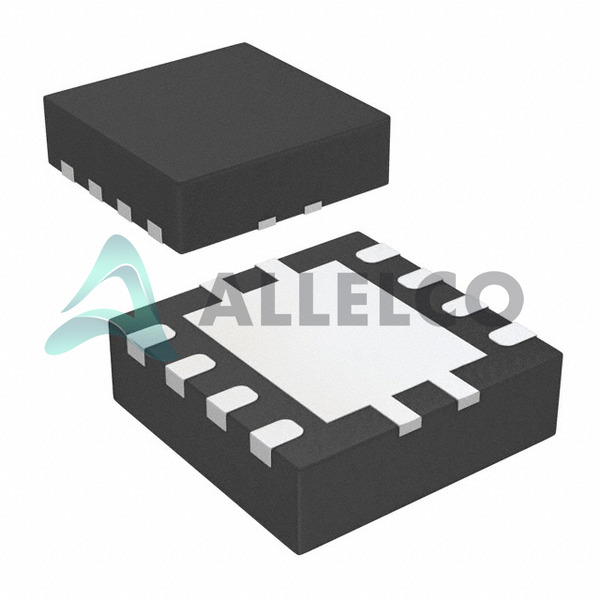
Surface Mount, 8-VDFN Exposed Pad packaging supports compact PCB designs

Application Areas

Automotive systems

Consumer electronics

Industrial automation

Telecommunication devices

Power management solutions

Product Lifecycle

Active status, indicating ongoing production and availability

Details on discontinuation or upcoming upgrades are not specified, suggesting stable supply for the foreseeable future

Several Key Reasons to Choose This Product

High efficiency and reliability from a leading manufacturer, Texas Instruments

Low drop-out and low quiescent current optimize power usage

Comprehensive protection features ensure safety and durability

Versatile for a wide range of applications due to stable 1.2V output and compatibility

Active product lifecycle status ensures long-term availability and support

Frequently Asked Questions(FAQ)

What are the key thermal and electrical trade-offs when using the TPS7A8012DRBR in a compact 8-SON (3x3) package for a 1A load application?
The TPS7A8012DRBR delivers 1A output current in a thermally efficient 8-SON (3x3) package with an exposed pad, enabling good heat dissipation when properly soldered to a PCB ground plane. However, at full load and high input-output differentials—such as 5V input to 1.2V output—power dissipation reaches 3.8W, which demands careful thermal layout. The junction temperature must stay within the -40°C to 125°C range; without adequate copper area or airflow, localized heating may trigger thermal shutdown. Engineers should allocate at least 200 mm² of 2 oz copper connected to the exposed pad to maintain safe operating temperatures under sustained load.
How does the dropout voltage of the TPS7A8012DRBR compare to other 1A LDOs, and what input headroom is required for stable 1.2V regulation?
The TPS7A8012DRBR has a maximum dropout voltage of 0.5V at 1A load, meaning the input voltage must remain above 1.7V to maintain regulation. This is competitive among 1A fixed-output LDOs, though some ultra-low-dropout alternatives achieve sub-200 mV dropout at lower currents. For battery-powered systems where input voltage sags near end-of-life, this 0.5V margin may limit usable capacity. Designers should verify that the upstream supply, including DC-DC converter ripple or battery discharge curves, consistently exceeds 1.7V under worst-case load conditions.
Can the TPS7A8012DRBR be used in reverse polarity scenarios, and how does its protection circuitry respond?
Yes, the TPS7A8012DRBR includes reverse polarity protection, which prevents damage if the input and ground are accidentally swapped. This feature is particularly valuable in industrial or automotive prototyping environments where incorrect wiring may occur. The internal circuitry clamps reverse voltages and blocks current flow, protecting both the regulator and downstream components. However, this protection is not a substitute for proper input filtering or external diodes in high-reliability applications—it is designed for fault tolerance, not continuous reverse operation.
What is the significance of the 120 µA quiescent current in the TPS7A8012DRBR for battery-operated systems?
With a quiescent current of 120 µA, the TPS7A8012DRBR is suitable for low-power applications such as IoT sensors or portable devices where standby efficiency matters. While not ultra-low-Iq (some modern LDOs operate below 10 µA), this level is reasonable for systems with moderate sleep currents. For example, in a device drawing 100 µA in sleep mode, the regulator’s own Iq contributes significantly to total drain. Designers should evaluate whether a switching regulator might offer better system-level efficiency if the load profile includes long idle periods.
How does the PSRR performance of the TPS7A8012DRBR impact noise-sensitive analog circuits downstream?
The TPS7A8012DRBR provides 48dB of power supply rejection at 100Hz, decreasing to 38dB at 1MHz, which is adequate for moderate noise environments but may not suffice for high-precision ADCs or RF stages without additional filtering. In mixed-signal designs, switching regulators upstream can introduce ripple above 100kHz; while the LDO attenuates this, residual noise may still affect sensitive rails. Engineers should consider adding a small ceramic capacitor (e.g., 1 µF X7R) at the output and possibly an LC filter at the input when powering precision analog loads.
What design considerations apply when paralleling multiple TPS7A8012DRBR devices to increase current capacity?
The TPS7A8012DRBR is not designed for current sharing via direct paralleling due to lack of active load balancing and slight output voltage tolerances. Even minor mismatches in output voltage can cause one device to carry disproportionate current, leading to thermal runaway. If higher than 1A is needed, a single higher-current regulator or a dedicated current-sharing controller should be used instead. For redundancy or distributed power, separate regulators with individual feedback networks are preferred.
How does the enable function on the TPS7A8012DRBR support power sequencing in multi-rail systems?
The enable pin on the TPS7A8012DRBR allows precise control of power-up timing, enabling coordination with other voltage rails in FPGA or processor-based systems. With a typical turn-on threshold around 1.2V, it can be driven directly by microcontroller GPIOs or power management ICs. When disabled, the output discharges through internal circuitry, minimizing residual voltage. This feature supports sequencing protocols where core logic (e.g., 1.2V) must power up after I/O rails, reducing inrush current and latch-up risk.
What are the reliability implications of the MSL-1 rating for the TPS7A8012DRBR in high-volume manufacturing?
The moisture sensitivity level (MSL) of 1 (unlimited floor life) for the TPS7A8012DRBR simplifies handling and storage in production environments. Unlike higher MSL components that require dry packing and strict bake protocols, this device can be exposed to ambient conditions indefinitely before reflow, reducing logistical overhead and risk of moisture-induced defects during soldering. This is particularly advantageous in high-mix manufacturing where inventory turnover varies.
How does the TPS7A8012DRBR compare to the TPS7A8012DRBT variant, and when would one be preferred over the other?
The TPS7A8012DRBR and TPS7A8012DRBT are functionally identical, differing only in packaging format—DRBR is tape and reel (TR), while DRBT is typically cut tape or tray. For automated SMT assembly lines, DRBR is preferred due to compatibility with pick-and-place feeders. Manual prototyping or low-volume builds may use DRBT for easier handling. Electrical performance, pinout, and thermal characteristics remain unchanged between the two.
What input and output capacitor values are recommended for stable operation of the TPS7A8012DRBR, and what happens if they are omitted?
Texas Instruments specifies a minimum 2.2 µF ceramic capacitor (X5R or X7R, 6.3V rating or higher) on both input and output for stability of the TPS7A8012DRBR. These capacitors ensure loop stability and suppress transient responses. Omitting them—or using capacitors with high ESR—can lead to oscillations, especially under fast load steps. In practice, a 4.7 µF output capacitor improves transient response for digital loads with sharp current demands, such as microcontrollers during wake-up events.
Can the TPS7A8012DRBR operate reliably at its maximum junction temperature of 125°C in enclosed environments?
The TPS7A8012DRBR is rated for operation up to 125°C junction temperature, but sustained operation near this limit reduces long-term reliability due to electromigration and oxide degradation. In enclosed or high-ambient-temperature systems (e.g., industrial enclosures), thermal derating is essential. For example, at 85°C ambient, even moderate power dissipation can push the junction close to its limit without sufficient copper area. Designers should use thermal simulation or empirical testing to validate margin under worst-case conditions.
How does the UVLO feature in the TPS7A8012DRBR protect the system during brownout conditions?
The under-voltage lockout (UVLO) in the TPS7A8012DRBR prevents erratic behavior by disabling the output when the input voltage falls below a threshold (typically around 2.5V, though exact value depends on internal bandgap). This ensures that downstream logic does not operate in an undefined state during power-up, shutdown, or brownouts. For systems with unstable input sources—such as solar-powered nodes or aging batteries—this feature enhances reliability by guaranteeing clean power transitions.
Is the TPS7A8012DRBR suitable for post-regulation after a switching converter in a noise-critical application?
Yes, the TPS7A8012DRBR can serve as an effective post-regulator after a DC-DC converter, leveraging its PSRR to clean up switching noise. For instance, when placed after a 5V buck converter to generate a clean 1.2V rail for a processor core, it attenuates high-frequency ripple that could otherwise couple into sensitive digital logic. However, the overall efficiency will be lower than a dedicated low-noise switching solution, so this approach is best when noise performance outweighs efficiency concerns.
What layout practices are critical for maximizing performance of the TPS7A8012DRBR in a 2-layer PCB design?
In a 2-layer board, thermal and electrical performance of the TPS7A8012DRBR hinges on proper grounding and copper pour. The exposed pad must be soldered to a solid ground plane with multiple vias (at least 4–6) to transfer heat to the bottom layer. Input and output capacitors should be placed within 2–3 mm of their respective pins to minimize loop inductance. Avoid routing high-current traces under the device, and ensure the feedback path (though internal for fixed output) remains uncontaminated by digital noise.

Parts with Similar Specifications

The three parts on the right have similar specifications to Texas Instruments TPS7A8012DRBR

Product Attribute TPS7A8018DRBR TPS7A8001DRBR TPS7A8012DRBT TPS7A8050DRBR
Part Number TPS7A8018DRBR TPS7A8001DRBR TPS7A8012DRBT TPS7A8050DRBR
Manufacturer Texas Instruments Texas Instruments Texas Instruments Texas Instruments
PSRR - - - -
Output Configuration - - - -
Output Type - Current - Unbuffered Voltage - Buffered -
Mounting Type - Surface Mount Through Hole Surface Mount
Operating Temperature - -40°C ~ 85°C 0°C ~ 70°C -40°C ~ 85°C
Current - Output - - - -
Number of Regulators - - - -
Control Features - - - -
Package / Case - 196-LFBGA 16-DIP (0.300', 7.62mm) 64-VFQFN Exposed Pad
Base Product Number - DAC34H84 MAX500 ADS62P42
Voltage - Input (Max) - - - -
Voltage - Output (Min/Fixed) - - - -
Series - - - -
Current - Quiescent (Iq) - - - -
Current - Supply (Max) - - - -
Package - Tape & Reel (TR) Tube Tape & Reel (TR)
Voltage Dropout (Max) - - - -
Protection Features - - - -
Supplier Device Package - 196-NFBGA (12x12) 16-PDIP 64-VQFN (9x9)
Voltage - Output (Max) - - - -

TPS7A8012DRBR Datasheet PDF

Download TPS7A8012DRBR pdf datasheets and Texas Instruments documentation for TPS7A8012DRBR - Texas Instruments.

Datasheets
LDOs Quick Reference Guide.pdf
HTML Datasheet
TPS7A80xx Datasheet.pdf

Customer Reviews

Evaluation: 10 Articles

  • Dani***alkerTech
    Jun 1, 2026

    Product works, but setup took more effort than expected. Once configured the MCU ran reliably, although documentation support felt older compared with newer platforms. Fine for maintenance projects.

  • Yuki***aka88
    May 26, 2026

    信号通信プロジェクトでこのRS-485トランシーバーを使用しました。設置は簡単で、長距離ケーブルでも通信は安定していました。消費電力も、以前使用していたものより低くなっています。

  • Stev***aker
    May 20, 2026

    Solid diode for power rectification. Works well in switching circuits.

  • Bran***Lewis
    May 11, 2026

    Compact FPGA with good performance. Suitable for basic signal processing tasks.

  • Oliv***arris
    May 7, 2026

    Reliable I/O expander. Works well in embedded control applications.

  • Jess***Jones
    Apr 17, 2026

    It offers good value for the price, and the specifications match the description. I’ve been using it for two days with no issues, and I’ll definitely buy it again if I need it in the future.

  • Mich***Smith
    Apr 17, 2026

    Shipping was on time, the component pins are neatly aligned, and I tested 10 of them with a multimeter—all readings were within the specified range. Highly recommended.

  • Aman***arris
    Apr 3, 2026

    It was great—the entire process, from placing the order to receiving the package, went very smoothly. The components were consistent, the price was fair, and I had a very pleasant shopping experience.

  • Mike***nch
    Apr 3, 2026

    Better than expected! The resistance and capacitance readings were spot-on, and it passed the test on the first try. The service was reliable, and the packaging was thoughtful—I highly recommend it.

  • Daic***K.
    Mar 23, 2026

    Very good. No issue after long time testing.

Write a Review

Your Email address will not be published.

Shipment

Delivery Time

In-stock items can be shipped within 24 hours. Some parts will be arranged for delivery within 1-2 days from the date all items arrive at our warehouse. And Allelco ships order once a day at about 17:00, except Sunday. Once the goods are shipped, the estimated delivery time depends on the shipping methods and Delivery destination. The table below shows are the logistic time for some common countries.

Delivery Cost

  1. Use your express account for shipment if you have one.
  2. Use our account for the shipment. Refer to the table below for the approximate charges.
(Different time frame / countries / package size has different price.)

Delivery Method

  1. Global Common Shipment by DHL / UPS / FedEx / TNT / EMS / SF we support.
  2. Others more shipping ways, please get in touch with your customer manager.

Common Countries Logistic Time Reference
Region Country Logistic Time(Day)
America United States 5
Brazil 7
Europe Germany 5
United Kingdom 4
Italy 5
Oceania Australia 6
New Zealand 5
Asia India 4
Japan 4
Middle East Israel 6
DHL & FedEx Shipment Charges Reference
Shipment charges(KG) Reference DHL(USD$)
0.00kg-1.00kg USD$30.00 - USD$60.00
1.00kg-2.00kg USD$40.00 - USD$80.00
2.00kg-3.00kg USD$50.00 - USD$100.00
Note:
The above table is for reference only. There may have some data bias for the uncontrollable factors.
Contact us if you have any questions.
  • QC (Quality Warranty)
  • Payment Support
  • Packaging
  • Certifications & Memberships

QC (Quality Warranty)

Allelco is committed to exceeding customer expectations through customer service excellence, order accuracy, and on-time delivery.
This is achieved through our commitment to the continual improvement of our processes, services, and products.


Strict quality inspection builds a solid foundation for electronic component quality.
  1. Visual inspection
  2. Performance testing and reliability verification
  3. Standardized full-process testing
  4. Precise control of every parameter
We eliminate defective components and ensure the stable operation of electronic devices through professional quality standards.

Payment Support

The payment method can be chosen from the methods shown below: Wire Transfer (T/T, Bank Transfer), Western Union, Credit card, PayPal.
  • HKBea
  • Paypal
  • MasterCard
  • Western-Union
  • VISA
Stable Delivery, Sincere Partnership — Your Faithful Supply Chain Partner
  • Efficient Supply Management
  • Cost-Saving Procurement
  • Fast Sourcing & Delivery
Contact us if you have any questions.

Packaging

Electrostatic Discharge Protection and Handling

All electrostatic-sensitive components are handled in accordance with electrostatic discharge control procedures. The products are hermetically sealed in anti-static safe packaging to prevent electrostatic damage. Appropriate labeling is also applied for identification and traceability. This ensures product integrity during storage, handling and transportation.


ESD

Certifications & Memberships

Third-party certified, strict quality control. Our certification
  • ISO 9001: 2015
  • ISO 13485: 2016
  • ISO 14001: 2015
  • ISO 28000: 2007
  • ISO 45001: 2018
  • GB/T 27922-2011
  • SMTA
  • IPC
  • ESD
  • PSMA
TPS7A8012DRBR Image

TPS7A8012DRBR

Texas Instruments
32D-TPS7A8012DRBR

Want a better price? Add to Cart and Submit RFQ now, we'll contact you immediately.

0 RFQ
Shopping cart (0 Items)
It is empty.
Compare List (0 Items)
It is empty.
Feedback

Your feedback matters! At Allelco, we value the user experience and strive to improve it constantly.
Please share your comments with us via our feedback form, and we'll respond promptly.
Thank you for choosing Allelco.

Subject
E-mail
Comments
Captcha
Drag or click to upload file
Upload File
types: .xls, .xlsx, .doc, .docx, .jpg, .png and .pdf.
Max file size: 10MB