
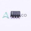

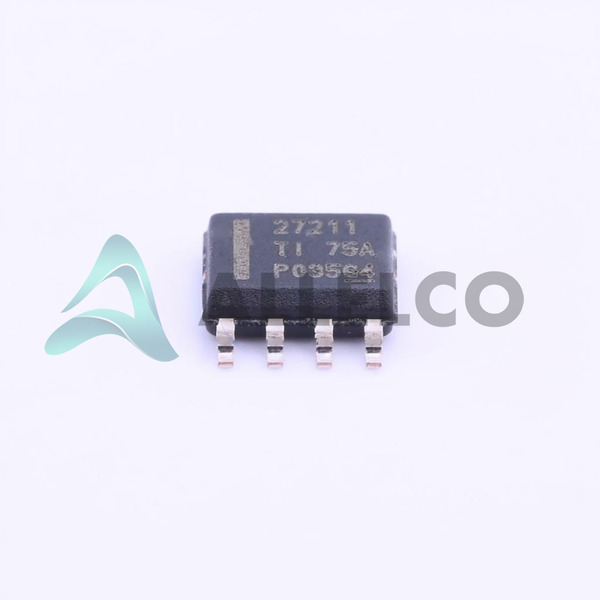
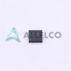
UCC27211DDAR (1)
Manufacturer Part Number
UCC27211DDAR
Manufacturer
Texas Instruments
Introduction
The UCC27211DDAR from Texas Instruments is a high-performance, half-bridge gate driver designed for efficient power management and signal amplification in a wide range of applications.
Product Features and Performance
Operates with supply voltages from 8V to 17V.
Provides independent driving for two N-Channel MOSFET gates.
Supports high-side voltages up to 120V via bootstrap technique.
Delivers peak output currents of 4A for both source and sink.
Features fast rise and fall times of 7.2ns and 5.5ns, respectively.
Input type is non-inverting for straightforward signal processing.
Engineered with robust thermal performance, operating between -40°C and 140°C (TJ).
Product Advantages
Allows for efficient switching performance, reducing power losses.
Enhances signal integrity and responsiveness due to quick rise/fall times.
Enables flexible design options with its wide range of operating voltages.
Supports high current driving capabilities for demanding applications.
Offers high reliability and long operational lifespan in extreme conditions.
UCC27211DDAR (2)
Key Technical Parameters
Driven Configuration: Half-Bridge
Channel Type: Independent
Number of Drivers: 2
Gate Type: N-Channel MOSFET
Supply Voltage: 8V ~ 17V
Logic Voltage VIL, VIH: 1.3V, 2.8V
Peak Output Current: 4A (Source), 4A (Sink)
High Side Voltage Max (Bootstrap): 120V
Rise/Fall Time (Typ): 7.2ns/5.5ns
Quality and Safety Features
Manufactured by Texas Instruments, a leader in semiconductor innovation.
Constructed with high-quality materials for durability and long-term reliability.
Strict quality control processes ensure that each unit meets high safety standards.
Compatibility
Compatible with a wide range of N-Channel MOSFETs.
Flexible for use in various circuit designs due to its non-inverting input type.
Application Areas
Power supplies
Motor controls
Inductive load switching
High-frequency power converters
Product Lifecycle
This product is currently in Active status, indicating ongoing production and availability.
No information suggests nearing discontinuation, ensuring long-term supply for designs.
Several Key Reasons to Choose This Product
High-performance characteristics suitable for demanding power management tasks.
Fast switching speeds improve efficiency and reduce thermal load.
Versatile voltage and current handling capabilities support a broad range of applications.
Developed and supported by Texas Instruments, assuring quality and reliability.
Availability in Tape & Reel packaging facilitates efficient assembly processes for high-volume production.

 UCC27211ADRMRTexas InstrumentsIC GATE DRVR HALF-BRIDGE 8VSON
 UCC27211ADRMTTexas InstrumentsIC GATE DRVR HALF-BRIDGE 8VSON
 UCC27211DTexas InstrumentsIC GATE DRVR HALF-BRIDGE 8SOIC
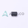 UCC27211DRTexas InstrumentsIC GATE DRVR HALF-BRIDGE 8SOIC
 UCC27211ADTexas InstrumentsHALF BRIDGE BASED MOSFET DRIVER
 UCC27212DPRTTexas InstrumentsIC GATE DRVR HALF-BRIDGE 10WSON
 UCC27211DRMTTexas InstrumentsIC GATE DRVR HALF-BRIDGE 8VSON
 UCC27212DPRRTexas InstrumentsIC GATE DRVR HALF-BRIDGE 10WSON
 UCC27211ADDARTexas Instruments


