
Manufacturer Part Number
ADC104S051CIMM/NOPB
Manufacturer
Texas Instruments
Introduction
The ADC104S051CIMM/NOPB is a high-performance, low-power 10-bit analog-to-digital converter (ADC) with four input channels. It features a successive approximation register (SAR) architecture, offering fast conversion rates, low power consumption, and a simple serial interface.
Product Features and Performance
10-bit resolution
500 kSPS sampling rate
4 single-ended input channels
SAR architecture for fast conversion
Low power consumption
SPI/DSP-compatible serial interface
Product Advantages
High sampling rate for demanding applications
Low power consumption for battery-operated devices
Compact 10-TFSOP/10-MSOP package
Key Reasons to Choose This Product
Excellent performance-to-power ratio
Versatile input configuration with 4 single-ended channels
Easy integration with microcontrollers and digital signal processors
Reliable and robust design from a trusted manufacturer
Quality and Safety Features
Industrial temperature range of -40°C to 85°C
Lead-free and RoHS-compliant construction
Compatibility
The ADC104S051CIMM/NOPB is compatible with a wide range of microcontrollers and digital signal processors supporting the SPI or DSP serial interface.
Application Areas
Industrial control systems
Portable and battery-powered devices
Instrumentation and measurement equipment
Automotive electronics
Medical devices
Product Lifecycle
The ADC104S051CIMM/NOPB is an active product, and Texas Instruments currently offers it as a standard part. There are no immediate plans for discontinuation, and customers can expect continued support and availability. If you have any questions or need assistance with alternative or equivalent models, please contact our sales team through our website.
 ADC104S051CIMMX/NOPBTexas InstrumentsIC ADC 10BIT SAR 10VSSOP
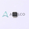 ADC104S021CIMMXTexas InstrumentsIC ADC 10BIT SAR 10VSSOP
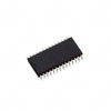 ADC10464CIWMX/NOPBTexas InstrumentsIC ADC 10BIT FLASH 28SOIC
 ADC1061CIN/NOPBTexas InstrumentsIC ADC 10BIT FLASH 20DIP
 ADC104S021QIMMTexas Instruments
 ADC1061CINNS


