
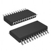
Manufacturer Part Number
TLC3548CDWR
Manufacturer
Texas Instruments
Introduction
The TLC3548CDWR is a high-performance, 14-bit analog-to-digital converter (ADC) with a sampling rate of up to 200kHz. It features a multi-channel input configuration, flexibility in reference voltage sources, and a SPI digital interface, making it suitable for a wide range of data acquisition and control applications.
Product Features and Performance
14-bit resolution
Sampling rate up to 200kSPS
4 or 8 input channels
Pseudo-differential and single-ended input types
SPI digital interface
Internal or external reference voltage
1:1 sample-and-hold to ADC architecture
Integrated multiplexer
Product Advantages
High-resolution data conversion
Flexible multi-channel input configuration
Compatibility with a variety of reference voltage sources
Efficient SPI digital interface for easy system integration
Optimal performance-to-power ratio
Key Reasons to Choose This Product
Reliable and high-performance data acquisition solution
Versatile input options to accommodate diverse application needs
Seamless integration with microcontrollers and other digital systems
Cost-effective and power-efficient design
Quality and Safety Features
Robust industrial-grade packaging and construction
Compliance with relevant safety and environmental standards
Extensive testing and quality control measures
Compatibility
Suitable for a wide range of industrial, medical, and consumer electronics applications
Compatible with various microcontrollers and digital systems supporting SPI interface
Application Areas
Industrial process control and automation
Medical instrumentation and patient monitoring
Consumer electronics and portable devices
Test and measurement equipment
Product Lifecycle
The TLC3548CDWR is currently in the Last Time Buy phase, which means it is nearing discontinuation. However, Texas Instruments may have equivalent or alternative models available. Customers are advised to contact our website's sales team for the latest product information and availability.
 TLC3548IDWTexas InstrumentsIC ADC 14BIT SAR 24SOIC
 TLC3545IDGKTexas InstrumentsIC ADC 14BIT SAR 8VSSOP
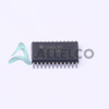 TLC3548IDWRTexas InstrumentsIC ADC 14BIT SAR 24SOIC
 TLC3545IDRTexas InstrumentsIC ADC 14BIT SAR 8SOIC
 TLC3548EVMTexas InstrumentsEVALUATION MODULE FOR TLC3548
 TLC3548CPWG4Luminary Micro / Texas InstrumentsIC ADC 14BIT 200KSPS 8CH 24TSSOP


