

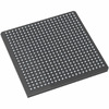
A3P1000L-FGG144I (1)
Manufacturer Part Number
A3P1000L-FGG144I
Manufacturer
Microchip Technology
Introduction
The A3P1000L-FGG144I is an embedded FPGA (Field Programmable Gate Array) from Microchip Technology's ProASIC3L series designed for versatile applications needing programmable logic solutions.
Product Features and Performance
Embedded FPGA with programmable logic
1 million gates capacity
97 programmable I/Os
Integrated 147,456 RAM bits for high-speed data processing
Surface mount 144-LBGA package
Operational across a wide voltage supply range from 1.14V to 1.575V
Works effectively in extreme temperature conditions ranging from -40°C to 100°C
Product Advantages
Low power consumption
Compact size suitable for space-constrained applications
High integration helps reduce the overall system cost
Robust operating temperature range enhances reliability
Key Technical Parameters
Total RAM Bits: 147456
Number of I/O: 97
Number of Gates: 1000000
Voltage Supply: 1.14V ~ 1.575V
Operating Temperature: -40°C ~ 100°C (TJ)
Quality and Safety Features
Built-in thermal management with a wide operating temperature range ensures component durability and safety under variable environmental conditions
Rigorous quality control conforms to industry standards for reliability and longevity
Compatibility
Compatible with various systems due to standardized 144-FPBGA packaging and typical FPGA interface features
Application Areas
Telecommunications
Consumer electronics
Automotive industry
Industrial automation
Data processing
Product Lifecycle
Status: Active
Not nearing discontinuation and has support for future upgrades or replacements available
Several Key Reasons to Choose This Product
Exceptional processing power with a million gate capacity for complex and intensive applications
Enhanced flexibility with 97 I/O options for various connection possibilities
Low power requirements make it ideal for power-sensitive applications
Thermal and operational reliability in varied environmental conditions ensures prolonged usability
Backed by Microchip Technology's robust support and product longevity assurance
 A3P1000L-PQ208IMicrosemi CorporationIC FPGA 154 I/O 208QFP
 A3P1000L-FG256Microchip TechnologyIC FPGA 177 I/O 256FBGA
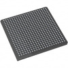 A3P1000L-FG484Microsemi CorporationIC FPGA 300 I/O 484FBGA
 A3P1000L-FGG256IMicrochip TechnologyIC FPGA 177 I/O 256FBGA
 A3P1000PQG208ACTEL


