
R7F7010243AFE#KA2 (1)
Manufacturer Part Number
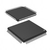
R7F7010243AFE#KA2
Manufacturer
renesas-electronics-america
Introduction
The R7F7010243AFE#KA2 is a powerful 32-bit single-core embedded microcontroller from Renesas Electronics America, designed for automotive applications. Built on the RH850/F1L series, it operates at a speed of 80MHz and incorporates a wide range of connectivity options and on-chip peripherals for enhanced performance and functionality.
Product Features and Performance
32-Bit Single-Core RH850G3K processor
Speed of 80MHz delivering robust performance
Advanced connectivity including CANbus, CSI, I2C, LINbus, SPI, UART/USART
Rich set of peripherals such as DMA, PWM, WDT
Program memory size of 768KB FLASH
Additional EEPROM size of 32K x 8 and RAM size of 96K x 8
Integrated A/D converters with 20x10b and 16x12b resolutions
Supported by an internal oscillator
Operating Temperature range of -40°C to 105°C
Surface Mount, 100-LFQFP (14x14) packaging
Product Advantages
Comprehensive connectivity options for flexible system communication
Large memory capacity for complex applications
Built-in digital and analog peripherals minimize the need for external components
Wide operating temperature range suitable for harsh environments
Surface mount packaging for compact design solutions
Key Technical Parameters
Core Size: 32-Bit
Speed: 80MHz
Program Memory: 768KB FLASH
EEPROM: 32K x 8
RAM: 96K x 8
Voltage Supply: 3V ~ 5.5V
A/D Converters: 20x10b, 16x12b
Operating Temperature: -40°C ~ 105°C
Package: 100-LQFP
Quality and Safety Features
Designed following industry standards for automotive applications
Enhanced reliability and performance under extended temperatures
Compatibility
Supports a wide range of automotive communication protocols
Compatible with various development tools for comprehensive development support
Application Areas
Automotive control units
Body control modules
Advanced driver assistance systems (ADAS)
Powertrain and engine management systems
Product Lifecycle
Current Product Status: Active
Not nearing discontinuation, ensuring long-term availability
Support for replacements or upgrades is available
Several Key Reasons to Choose This Product
High-performance core and extensive memory resources support complex automotive applications
Broad range of integrated peripherals reduces system costs and complexity
Flexibility in communication interfaces caters to various automotive networking requirements
Reliable operation under extreme conditions ensures suitability for automotive environments
Active product lifecycle status with Renesas' commitment to long-term support and availability


