View All

Please refer to the English Version as our Official Version.Return

Europe
France(Français) Germany(Deutsch) Italy(Italia) Russian(русский) Poland(polski) Czech(Čeština) Luxembourg(Lëtzebuergesch) Netherlands(Nederland) Iceland(íslenska) Hungarian(Magyarország) Spain(español) Portugal(Português) Turkey(Türk dili) Bulgaria(Български език) Ukraine(Україна) Greece(Ελλάδα) Israel(עִבְרִית) Sweden(Svenska) Finland(Svenska) Finland(Suomi) Romania(românesc) Moldova(românesc) Slovakia(Slovenská) Denmark(Dansk) Slovenia(Slovenija) Slovenia(Hrvatska) Croatia(Hrvatska) Serbia(Hrvatska) Montenegro(Hrvatska) Bosnia and Herzegovina(Hrvatska) Lithuania(lietuvių) Spain(Português) Switzerland(Deutsch) United Kingdom(English)
Asia/Pacific
Japan(日本語) Korea(한국의) Thailand(ภาษาไทย) Malaysia(Melayu) Singapore(Melayu) Vietnam(Tiếng Việt) Philippines(Pilipino)
Africa, India and Middle East
United Arab Emirates(العربية) Iran(فارسی) Tajikistan(فارسی) India(हिंदी) Madagascar(malaɡasʲ)
South America / Oceania
New Zealand(Maori) Brazil(Português) Angola(Português) Mozambique(Português)
North America
United States(English) Canada(English) Haiti(Ayiti) Mexico(español)
HomeProductsIntegrated Circuits (ICs)Embedded - MicrocontrollersSTM32F103RDY6TR
STM32F103RDY6TR Image
Image may be representation.
See specifications for product details.
EXPRESS OPTION
Payment method

STM32F103RDY6TR - STMicroelectronics

Manufacturer Part Number
STM32F103RDY6TR
Manufacturer
STMicroelectronics
Allelco Part Number
32D-STM32F103RDY6TR
Warranty
1 Year Allelco Warranty - Find out more
Stock Status:
4,742 pcs available, New & Original
Parts Description
IC MCU 32BIT 384KB FLASH 64WLCSP
Package
64-WLCSP (4.47×4.4)
Data sheet
STM32F103RDY6TR.pdf
RoHs Status
ROHS3 Compliant
Our certification
In stock: 4742
  • Unit Price: $12.83
  • Subtotal: $0.00

Want a better price?
Add to Cart and Submit RFQ now, we'll contact you immediately.

Quantity Unit Price Ext. Price
1+ $12.83 $12.83
30+ $12.29 $368.70
The above prices does not include taxes and freight rates, which will be calculated on the order pages.

Specifications

STM32F103RDY6TR Tech Specifications
STMicroelectronics - STM32F103RDY6TR technical specifications, attributes, parameters and parts with similar specifications to STMicroelectronics - STM32F103RDY6TR

Product Attribute Attribute Value
Manufacturer STMicroelectronics
Voltage - Supply (Vcc/Vdd) 2V ~ 3.6V
Supplier Device Package 64-WLCSP (4.47×4.4)
Speed 72MHz
Series STM32F1
RAM Size 64K x 8
Program Memory Type FLASH
Program Memory Size 384KB (384K x 8)
Peripherals DMA, Motor Control PWM, PDR, POR, PVD, PWM, Temp Sensor, WDT
Package / Case 64-UFBGA, WLCSP
Package Tape & Reel (TR)
Product Attribute Attribute Value
Oscillator Type Internal
Operating Temperature -40°C ~ 85°C (TA)
Number of I/O 51
Mounting Type Surface Mount
EEPROM Size -
Data Converters A/D 16x12b; D/A 2x12b
Core Size 32-Bit Single-Core
Core Processor ARM® Cortex®-M3
Connectivity CANbus, I²C, IrDA, LINbus, SPI, UART/USART, USB
Base Product Number STM32F103

Environmental & Export Classifications

ATTRIBUTE DESCRIPTION
RoHs Status ROHS3 Compliant
Moisture Sensitivity Level (MSL) 1 (Unlimited)
REACH Status REACH Unaffected
ECCN 3A991A2
HTSUS 8542.31.0001

Parts Introduction

STM32F103RDY6TR Image
STM32F103RDY6TR (1)

Manufacturer Part Number

STM32F103RDY6TR

Manufacturer

STMicroelectronics

Introduction

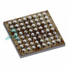
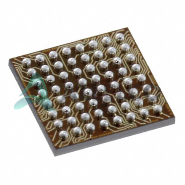
The STM32F103RDY6TR is a high-performance, ARM® Cortex®-M3 core-based microcontroller designed for embedded applications. It is part of STMicroelectronics’ STM32F1 series and comes in a 64-WLCSP package, optimized for cost-sensitive and space-constrained projects.

Product Features and Performance

32-Bit Single-Core ARM® Cortex®-M3 Processor

Speed of up to 72MHz

Advanced connectivity: CANbus, I2C, IrDA, LINbus, SPI, UART/USART, USB

Robust set of peripherals: DMA, Motor Control PWM, PDR (Power Down Reset), POR (Power On Reset), PVD (Programmable Voltage Detector), PWM (Pulse Width Modulation), Temp Sensor, WDT (Watchdog Timer)

Program Memory Size: 384KB (384K x 8) FLASH

RAM Size: 64K x 8

A/D 16x12b, D/A 2x12b converters for precise analog signal management

Internal Oscillator for reduced external component count

Operating Temperature range of -40°C to 85°C

Product Advantages

High integration level reduces external components and overall system costs

Flexible power supply (2V ~ 3.6V) compatibility supports energy-efficient designs

Extensive connectivity options enable complex applications

Comprehensive peripheral set supports varied application requirements without additional components

Large program memory and RAM facilitate sophisticated firmware development

Key Technical Parameters

Core: ARM® Cortex®-M3

Speed: 72MHz

Connectivity: CANbus, I2C, IrDA, LINbus, SPI, UART/USART, USB

Program Memory: 384KB FLASH

RAM: 64KB

Voltage Supply: 2V ~ 3.6V

Number of I/O: 51

Data Converters: A/D 16x12b, D/A 2x12b

Temperature Range: -40°C ~ 85°C

Quality and Safety Features

Includes Power On Reset (POR) and Power Down Reset (PDR) for enhanced safety and reliability

Programmable Voltage Detector (PVD) enables voltage monitoring for system protection

Integrated Watchdog Timer (WDT) prevents system hang-ups

Compatibility

Compatible with a wide range of external sensors and actuators due to its diverse connectivity options and numerous I/Os

Programmable in C/C++, ensuring ease of development with mainstream development tools

Application Areas

Industrial control systems

Motor control

Home automation

Sensor hubs

Medical devices

Embedded networking

Product Lifecycle

Status: Active

The STM32F103RDY6TR is not nearing discontinuation, ensuring long-term availability for ongoing and future projects

STMicroelectronics regularly provides updates and support

Several Key Reasons to Choose This Product

High processing power with a 32-bit ARM Cortex-M3 core

Extensive connectivity and peripheral set supports a broad range of applications

Efficient power consumption aids in designing energy-saving devices

Large memory capacity facilitates advanced application development

Robust set of quality and safety features enhance system reliability

Active product lifecycle status ensures long-term availability and support

Frequently Asked Questions(FAQ)

How does the STM32F103RDY6TR's power consumption compare to other STM32F1 series microcontrollers when operating at 72MHz with all peripherals active, and what design considerations are necessary for battery-powered applications?
The STM32F103RDY6TR typically draws approximately 36 mA during full-speed operation at 72MHz with the internal voltage regulator enabled and core voltage at 3.3V. Compared to lower-performance variants like the STM32F103C8T6, which consumes around 25–30 mA under similar conditions, the R variant offers more program memory (384KB vs. 64KB) and additional peripherals, resulting in higher but still efficient current draw. For battery-powered designs, engineers should consider enabling low-power modes such as Sleep or Stop mode via software configuration, using the internal voltage regulator only when necessary, and minimizing switching activity on high-capacitance loads. The device’s support for dynamic voltage scaling through the internal regulator allows trade-offs between performance and power, making it suitable for portable devices when paired with careful firmware optimization.
What are the key differences between the STM32F103RDY6TR and the STM32F103RCTx in terms of package size, pin count, and available I/O, especially for space-constrained PCB layouts?
The STM32F103RDY6TR is packaged in a 64-pin WLCSP (Wafer-Level Chip Scale Package) measuring 4.47×4.4 mm, offering 51 general-purpose I/O pins. In contrast, the STM32F103RCTx uses a 64-ball UFBGA package with identical pinout and functionality but larger footprint (~6×6 mm). While both share the same core processor and memory configuration, the WLCSP form factor of the R variant enables significantly reduced board area—ideal for compact consumer electronics. However, the WLCSP requires advanced soldering techniques (e.g., reflow with precise stencil alignment) and may not be compatible with standard pick-and-place equipment without specialized handling. Engineers selecting between them must balance assembly cost, thermal performance, and mechanical robustness against board real estate constraints.
Can the STM32F103RDY6TR reliably drive USB communication in a self-powered application, and what external components are required to meet USB 2.0 Full-Speed specifications?
Yes, the STM32F103RDY6TR supports USB 2.0 Full-Speed operation and can function as either a host or device in self-powered configurations. To meet electrical compliance, designers must include an external 1.5 kΩ pull-up resistor on D+ (for device mode) or D− (for low-speed peripheral emulation), along with a dedicated crystal oscillator of 12–16 MHz (typically 12 MHz) connected to OSC_IN/OSC_OUT. Additionally, a ferrite bead and bypass capacitors (e.g., 1 µF and 100 nF) near the VBUS pin are essential to filter noise. The internal 3.3V regulator must remain active during USB operation to ensure stable core voltage. Failure to implement these components correctly may result in enumeration failures or signal integrity issues, particularly in noisy industrial environments.
How does the internal temperature sensor in the STM32F103RDY6TR perform across its operating range, and what calibration strategy is recommended for accurate thermal monitoring in embedded systems?
The STM32F103RDY6TR includes an on-chip temperature sensor that provides a linear response within the -40°C to 85°C range. At room temperature (25°C), the sensor typically reads approximately 30–35 mV, corresponding to about +30°C offset due to process variations. This implies raw readings require calibration—ideally using factory-trimmed data if available from STMicroelectronics, or by performing two-point calibration at known reference temperatures (e.g., ambient and heated state). For most applications, a simple linear correction based on measured open-circuit voltage yields ±3°C accuracy without additional hardware. Implementing periodic sampling with ADC channel 16 ensures continuous thermal monitoring while minimizing CPU overhead.
What are the risks associated with using the STM32F103RDY6TR in automotive-grade environments, given its industrial temperature rating and lack of AEC-Q100 qualification?
Although the STM32F103RDY6TR operates from -40°C to 85°C, it is not qualified to AEC-Q100 standards and therefore carries elevated risk in automotive applications such as engine control units or infotainment systems where reliability demands are stringent. Extended thermal cycling, electromagnetic interference, and long-term drift under vibration may expose latent defects not covered by standard testing. While many non-automotive designs benefit from its robust peripherals and proven architecture, substituting this part for automotive requirements could lead to warranty claims, safety concerns, or failure in harsh operational profiles. Engineers should conduct rigorous environmental stress screening and consider alternative AEC-compliant parts like the STM32G4xx series if automotive certification is anticipated.
How does flash memory write endurance affect system longevity when using the STM32F103RDY6TR for frequent data logging, and what best practices minimize wear?
The STM32F103RDY6TR features 10,000 write cycles per flash page (typically 1 KB), meaning sustained writes to the same address will degrade memory over time. In data-logging applications writing 100 bytes every minute, this translates to ~17 hours of continuous operation before reaching theoretical limits—though practical lifespan extends further due to erase-before-write behavior and wear leveling not being native to the MCU. To extend usability, implement circular buffer logic across multiple sectors, avoid writing small fragments repeatedly, and reserve dedicated flash regions for critical parameters. Using EEPROM emulation in RAM or external FRAM reduces reliance on flash altogether, preserving integrity for decades-long deployments.
Is the STM32F103RDY6TR suitable for real-time motor control applications requiring encoder feedback, and how do its PWM and timer resources support such use cases?
The STM32F103RDY6TR includes three general-purpose timers (TIM2–TIM4) and one advanced-control timer (TIM1), all supporting complementary PWM outputs with dead-time insertion—critical for half-bridge motor drivers. With 72 MHz clock speed, timer resolution reaches 13.9 ns (1/72 MHz), enabling precise speed control down to fractions of a RPM. Encoder inputs can be handled via TIxA/B pins with quadrature decoding logic in hardware, reducing CPU load. However, compared to higher-end STM32 lines like the F4 or G0 series, it lacks dedicated encoder interfaces and has fewer channels; thus, multi-axis systems may require external ICs or software-based decoding. For single-axis BLDC or stepper motors up to 1 kW, the R variant performs adequately with optimized interrupt-driven ISRs and proper current sensing feedback loops.
How does the supply voltage tolerance of the STM32F103RDY6TR impact brown-out protection settings, and what happens if VDD drops below 2.0V during normal operation?
The STM32F103RDY6TR specifies operation from 2.0V to 3.6V, but brown-out detection (BOD) thresholds are programmable at 2.1V, 2.4V, or 2.7V via option bytes. If VDD falls below the selected threshold, the MCU resets automatically to prevent erratic behavior from undervoltage conditions. Operating below 2.0V risks latch-up or permanent damage, especially if I/O voltages exceed absolute maximum ratings. Designers should ensure input signals remain within 0–VDD range and add bulk capacitance (≥10 µF) near VDD pins to handle transient dips. In battery-powered systems, selecting a BOD level just above expected minimum voltage (e.g., 2.4V for Li-ion cutoff) balances stability with headroom for regulation losses.
What are the implications of using the STM32F103RDY6TR in wireless sensor nodes employing sub-1 GHz RF modules, considering its lack of integrated RF shielding and limited GPIO slew rate control?
The STM32F103RDY6TR does not include built-in RF shielding or filtering, so coexistence with sub-1 GHz transceivers (e.g., SX1276) demands careful PCB layout: keep analog and digital grounds separate, route RF traces away from clock lines, and use guard rings around sensitive nodes. Additionally, the GPIO output slew rates are fixed unless modified via APB registers, potentially causing electromagnetic emissions during high-frequency switching. While acceptable for moderate-speed SPI/I2C links, rapid toggling near RF bands can induce coupling. Engineers should validate EMC compliance early using spectrum analyzers and consider adding RC filters or ferrite chokes on control lines. Firmware-wise, scheduling RF transmissions during idle MCU states minimizes crosstalk.
How does the internal clock calibration mechanism work in the STM32F103RDY6TR, and why might users observe timing drift when relying solely on the internal 8 MHz RC oscillator?
The STM32F103RDY6TR employs a factory-calibrated internal 8 MHz RC oscillator (±1% typical, up to ±5% worst-case), which can be used directly or multiplied by 9 via PLL to generate the 72 MHz system clock. Without external trimming, temperature changes and silicon variations cause frequency drift exceeding 100 ppm/°C, leading to cumulative errors in UART baud rates, PWM duty cycles, or timing-critical tasks. For applications requiring <0.1% accuracy (e.g., motor commutation, audio generation), an external crystal (e.g., 8–16 MHz) with matched load capacitors is strongly advised. Alternatively, periodic re-calibration using a precision reference (like a GPS pulse-per-second signal) can correct drift dynamically, though this adds complexity.
What precautions are necessary when bootloading the STM32F103RDY6TR over UART, and how does its ROM bootloader interact with user code stored in flash?
Entering UART bootloader mode requires pulling BOOT0 to VDD while resetting the device—this activates the built-in ROM bootloader, which checks for valid command packets before erasing or programming flash. Critical precautions include ensuring stable power during transfer (brownouts corrupt data), disabling interrupts during flash operations, and verifying checksums post-write. The ROM loader supports only specific baud rates (e.g., 9600, 115200) and packet formats; mismatched settings cause timeouts. Importantly, the bootloader reserves the first 1 KB of flash for itself, so user applications must start above address 0x08000400. Corrupting the option byte configuration (especially read protection bits) may brick the device, necessitating SWIM recovery via ST-Link or similar programmer.
How does the STM32F103RDY6TR handle simultaneous access to flash memory during execution and programming, and what latency penalties occur when mixing code fetch with write operations?
Due to Harvard architecture with separated instruction and data buses, the STM32F103RDY6TR can execute code from flash while simultaneously reading/writing data, but flash programming halts instruction fetches for 15–20 cycles per page erase or 8 cycles per word write. During these windows, CPU stalls reduce effective throughput by up to 20% in worst-case scenarios (e.g., tight loops accessing constants). To mitigate, align critical code sections to 256-byte boundaries using scatter files, relocate frequently used routines to RAM via bootloader or startup scripts, and batch flash updates during idle periods. Note that dual-bank flash architectures (not present here) would eliminate this issue entirely, highlighting a limitation of older STM32F1 designs versus newer generations.
What are the thermal characteristics of the STM32F103RDY6TR in WLCSP packaging, and how does junction-to-ambient resistance affect heat dissipation in densely populated boards?
As a WLCSP device, the STM32F103RDY6TR lacks traditional leads, relying instead on solder bumps for conduction. Thermal impedance (ΘJA) is approximately 45°C/W under natural convection, implying a 1W power dissipation raises die temperature by 45°C above ambient. In practice, most designs dissipate far less than 1W (typically <0.5W), keeping junction temperatures manageable below 85°C even in enclosed spaces. However, adjacent high-power components or poor copper pour beneath the package can elevate local ambient temperature, reducing margin. Engineers should allocate sufficient ground plane area underneath the WLCSP, avoid placing it near heat sources, and verify thermal performance through IR imaging or long-term burn-in tests in target enclosures.
How does DMA configuration impact real-time performance when using the STM32F103RDY6TR for ADC sampling with UART transmission, and what pitfalls arise from misaligned buffer addresses?
The STM32F103RDY6TR supports DMA channels for both ADC and USART, enabling zero-CPU-transfer data movement. Properly configured, DMA allows continuous 12-bit ADC sampling at up to 1 Msps with automatic UART FIFO filling, maintaining deterministic latency. However, misaligned buffers (not divisible by 4 bytes) cause DMA faults or silent data corruption. Additionally, overlapping DMA requests without priority arbitration may starve lower-priority peripherals—especially problematic when CANbus transmits during ADC conversions. Best practice includes aligning buffers to word boundaries, using double-buffering for streaming data, and setting DMA priorities conservatively. Misconfiguration often manifests as intermittent data loss rather than crashes, making debugging challenging without logic analyzers.
What alternatives exist if the STM32F103RDY6TR cannot meet required peripheral count or memory needs, and how does stepping to the STM32F103RETx improve upon its limitations?
If 384KB flash or 51 I/Os are insufficient, upgrading to the STM32F103RETx (same LQFP-64 package) offers identical core specs but increases flash to 512KB and retains full peripheral suite, including extra timers and enhanced PWM capabilities. Unlike the R variant, however, the E version maintains conventional ball-grid packaging, simplifying assembly and inspection. Both share the same 72 MHz ARM Cortex-M3 core and 2–3.6V supply, ensuring software compatibility. The primary trade-off is cost and board space—the RETx uses larger package but matches pinout, allowing drop-in replacement in existing designs with minimal BOM change. For new projects demanding >384KB code storage or additional analog comparators, stepping up is advisable despite negligible firmware migration effort.
How does the STM32F103RDY6TR support secure firmware updates, and what hardware-level protections exist against unauthorized code injection?
The STM32F103RDY6TR implements basic read/write protection via option bytes: setting RDP (Read Protection) Level 1 disables flash readout, while WRP (Write Protection) locks specific sectors. Though not equivalent to modern TrustZone or Secure Boot, these mechanisms deter casual tampering. For secure updates, developers must integrate cryptographic verification (e.g., SHA-256 + RSA) in application code before flashing, ideally using a secondary bootloader in protected ROM. Without tamper-resistant packaging or hardware crypto accelerators (absent in F1 series), physical access remains a vector for extraction. Thus, secure update protocols depend entirely on software implementation, making side-channel attack mitigation and encrypted payloads essential for compliance-sensitive domains like medical devices.
What is the expected MTBF (Mean Time Between Failures) for the STM32F103RDY6TR in industrial control applications, and how do environmental factors influence reliability estimates?
Based on JEDEC JESD22-A104 accelerated life testing and typical usage profiles, the STM32F103RDY6TR achieves MTBF exceeding 1 million hours under controlled lab conditions (-40°C to 85°C, 50% humidity). However, real-world reliability degrades with thermal cycling (ΔT > 60°C/day), mechanical shock (>100g), or prolonged operation near 85°C ambient. Field data suggests failure rates increase exponentially beyond 70°C due to electromigration in bond wires and solder joints. For mission-critical systems, derating power consumption by 30%, avoiding hot spots via airflow management, and selecting conformal-coated PCBs enhance longevity. While not warrantied for 20-year lifecycles out-of-box, careful design can push operational life well beyond 10 years in benign environments.

Parts with Similar Specifications

The three parts on the right have similar specifications to STMicroelectronics STM32F103RDY6TR

Product Attribute STM32F103REY6TR STM32F103RDT6TR STM32F103RCY6TR STM32F103RCY6CTR
Part Number STM32F103REY6TR STM32F103RDT6TR STM32F103RCY6TR STM32F103RCY6CTR
Manufacturer STMicroelectronics STMicroelectronics STMicroelectronics STMicroelectronics
Oscillator Type - - - -
Series - - - -
Operating Temperature - -40°C ~ 85°C 0°C ~ 70°C -40°C ~ 85°C
Base Product Number - DAC34H84 MAX500 ADS62P42
Connectivity - - - -
Speed - - - -
Package / Case - 196-LFBGA 16-DIP (0.300', 7.62mm) 64-VFQFN Exposed Pad
Mounting Type - Surface Mount Through Hole Surface Mount
Supplier Device Package - 196-NFBGA (12x12) 16-PDIP 64-VQFN (9x9)
Core Size - - - -
Package - Tape & Reel (TR) Tube Tape & Reel (TR)
Data Converters - - - -
Core Processor - - - -
Program Memory Size - - - -
Voltage - Supply (Vcc/Vdd) - - - -
EEPROM Size - - - -
Number of I/O - - - -
RAM Size - - - -
Peripherals - - - -
Program Memory Type - - - -

STM32F103RDY6TR Datasheet PDF

Download STM32F103RDY6TR pdf datasheets and STMicroelectronics documentation for STM32F103RDY6TR - STMicroelectronics.

PCN Assembly/Origin
WLCSP Backend Assembly Add 28/Dec/2017.pdf

Customer Reviews

Evaluation: 10 Articles

  • Nath***rooks
    Jun 11, 2026

    Installed this power component in a converter board. Output remained stable under different load conditions and thermal performance was better than expected.

  • Dani***alkerTech
    Jun 1, 2026

    Product works, but setup took more effort than expected. Once configured the MCU ran reliably, although documentation support felt older compared with newer platforms. Fine for maintenance projects.

  • Yuki***aka88
    May 26, 2026

    信号通信プロジェクトでこのRS-485トランシーバーを使用しました。設置は簡単で、長距離ケーブルでも通信は安定していました。消費電力も、以前使用していたものより低くなっています。

  • Stev***aker
    May 20, 2026

    Solid diode for power rectification. Works well in switching circuits.

  • Bran***Lewis
    May 11, 2026

    Compact FPGA with good performance. Suitable for basic signal processing tasks.

  • Oliv***arris
    May 7, 2026

    Reliable I/O expander. Works well in embedded control applications.

  • Jess***Jones
    Apr 17, 2026

    It offers good value for the price, and the specifications match the description. I’ve been using it for two days with no issues, and I’ll definitely buy it again if I need it in the future.

  • Mich***Smith
    Apr 17, 2026

    Shipping was on time, the component pins are neatly aligned, and I tested 10 of them with a multimeter—all readings were within the specified range. Highly recommended.

  • Aman***arris
    Apr 3, 2026

    It was great—the entire process, from placing the order to receiving the package, went very smoothly. The components were consistent, the price was fair, and I had a very pleasant shopping experience.

  • Mike***nch
    Apr 3, 2026

    Better than expected! The resistance and capacitance readings were spot-on, and it passed the test on the first try. The service was reliable, and the packaging was thoughtful—I highly recommend it.

Write a Review

Your Email address will not be published.

Shipment

Delivery Time

In-stock items can be shipped within 24 hours. Some parts will be arranged for delivery within 1-2 days from the date all items arrive at our warehouse. And Allelco ships order once a day at about 17:00, except Sunday. Once the goods are shipped, the estimated delivery time depends on the shipping methods and Delivery destination. The table below shows are the logistic time for some common countries.

Delivery Cost

  1. Use your express account for shipment if you have one.
  2. Use our account for the shipment. Refer to the table below for the approximate charges.
(Different time frame / countries / package size has different price.)

Delivery Method

  1. Global Common Shipment by DHL / UPS / FedEx / TNT / EMS / SF we support.
  2. Others more shipping ways, please get in touch with your customer manager.

Common Countries Logistic Time Reference
Region Country Logistic Time(Day)
America United States 5
Brazil 7
Europe Germany 5
United Kingdom 4
Italy 5
Oceania Australia 6
New Zealand 5
Asia India 4
Japan 4
Middle East Israel 6
DHL & FedEx Shipment Charges Reference
Shipment charges(KG) Reference DHL(USD$)
0.00kg-1.00kg USD$30.00 - USD$60.00
1.00kg-2.00kg USD$40.00 - USD$80.00
2.00kg-3.00kg USD$50.00 - USD$100.00
Note:
The above table is for reference only. There may have some data bias for the uncontrollable factors.
Contact us if you have any questions.
  • QC (Quality Warranty)
  • Payment Support
  • Packaging
  • Certifications & Memberships

QC (Quality Warranty)

Allelco is committed to exceeding customer expectations through customer service excellence, order accuracy, and on-time delivery.
This is achieved through our commitment to the continual improvement of our processes, services, and products.


Strict quality inspection builds a solid foundation for electronic component quality.
  1. Visual inspection
  2. Performance testing and reliability verification
  3. Standardized full-process testing
  4. Precise control of every parameter
We eliminate defective components and ensure the stable operation of electronic devices through professional quality standards.

Payment Support

The payment method can be chosen from the methods shown below: Wire Transfer (T/T, Bank Transfer), Western Union, Credit card, PayPal.
  • HKBea
  • Paypal
  • MasterCard
  • Western-Union
  • VISA
Stable Delivery, Sincere Partnership — Your Faithful Supply Chain Partner
  • Efficient Supply Management
  • Cost-Saving Procurement
  • Fast Sourcing & Delivery
Contact us if you have any questions.

Packaging

Electrostatic Discharge Protection and Handling

All electrostatic-sensitive components are handled in accordance with electrostatic discharge control procedures. The products are hermetically sealed in anti-static safe packaging to prevent electrostatic damage. Appropriate labeling is also applied for identification and traceability. This ensures product integrity during storage, handling and transportation.


ESD

Certifications & Memberships

Third-party certified, strict quality control. Our certification
  • ISO 9001: 2015
  • ISO 13485: 2016
  • ISO 14001: 2015
  • ISO 28000: 2007
  • ISO 45001: 2018
  • GB/T 27922-2011
  • SMTA
  • IPC
  • ESD
  • PSMA
STM32F103RDY6TR Image

STM32F103RDY6TR

STMicroelectronics
32D-STM32F103RDY6TR

Want a better price? Add to Cart and Submit RFQ now, we'll contact you immediately.

0 RFQ
Shopping cart (0 Items)
It is empty.
Compare List (0 Items)
It is empty.
Feedback

Your feedback matters! At Allelco, we value the user experience and strive to improve it constantly.
Please share your comments with us via our feedback form, and we'll respond promptly.
Thank you for choosing Allelco.

Subject
E-mail
Comments
Captcha
Drag or click to upload file
Upload File
types: .xls, .xlsx, .doc, .docx, .jpg, .png and .pdf.
Max file size: 10MB