View All

Please refer to the English Version as our Official Version.Return

Europe
France(Français) Germany(Deutsch) Italy(Italia) Russian(русский) Poland(polski) Czech(Čeština) Luxembourg(Lëtzebuergesch) Netherlands(Nederland) Iceland(íslenska) Hungarian(Magyarország) Spain(español) Portugal(Português) Turkey(Türk dili) Bulgaria(Български език) Ukraine(Україна) Greece(Ελλάδα) Israel(עִבְרִית) Sweden(Svenska) Finland(Svenska) Finland(Suomi) Romania(românesc) Moldova(românesc) Slovakia(Slovenská) Denmark(Dansk) Slovenia(Slovenija) Slovenia(Hrvatska) Croatia(Hrvatska) Serbia(Hrvatska) Montenegro(Hrvatska) Bosnia and Herzegovina(Hrvatska) Lithuania(lietuvių) Spain(Português) Switzerland(Deutsch) United Kingdom(English)
Asia/Pacific
Japan(日本語) Korea(한국의) Thailand(ภาษาไทย) Malaysia(Melayu) Singapore(Melayu) Vietnam(Tiếng Việt) Philippines(Pilipino)
Africa, India and Middle East
United Arab Emirates(العربية) Iran(فارسی) Tajikistan(فارسی) India(हिंदी) Madagascar(malaɡasʲ)
South America / Oceania
New Zealand(Maori) Brazil(Português) Angola(Português) Mozambique(Português)
North America
United States(English) Canada(English) Haiti(Ayiti) Mexico(español)
HomeProductsIntegrated Circuits (ICs)Embedded - MicrocontrollersSTM32F215VGT6
STM32F215VGT6 Image
Image may be representation.
See specifications for product details.
EXPRESS OPTION
Payment method

STM32F215VGT6 - STMicroelectronics

Manufacturer Part Number
STM32F215VGT6
Manufacturer
STMicroelectronics
Allelco Part Number
32D-STM32F215VGT6
Warranty
1 Year Allelco Warranty - Find out more
Stock Status:
3,667 pcs available, New & Original
Parts Description
IC MCU 32BIT 1MB FLASH 100LQFP
Package
100-LQFP (14x14)
Data sheet
STM32F215VGT6.pdf
RoHs Status
ROHS3 Compliant
Our certification
In stock: 3667

Required fields are indicated by an asterisk (*)
Please send RFQ, we will respond immediately.

Quantity

Specifications

STM32F215VGT6 Tech Specifications
STMicroelectronics - STM32F215VGT6 technical specifications, attributes, parameters and parts with similar specifications to STMicroelectronics - STM32F215VGT6

Product Attribute Attribute Value
Manufacturer STMicroelectronics
Voltage - Supply (Vcc/Vdd) 1.8V ~ 3.6V
Supplier Device Package 100-LQFP (14x14)
Speed 120MHz
Series STM32F2
RAM Size 132K x 8
Program Memory Type FLASH
Program Memory Size 1MB (1M x 8)
Peripherals Brown-out Detect/Reset, DMA, I²S, LCD, POR, PWM, WDT
Package / Case 100-LQFP
Package Tray
Product Attribute Attribute Value
Oscillator Type Internal
Operating Temperature -40°C ~ 85°C (TA)
Number of I/O 82
Mounting Type Surface Mount
EEPROM Size -
Data Converters A/D 16x12b; D/A 2x12b
Core Size 32-Bit Single-Core
Core Processor ARM® Cortex®-M3
Connectivity CANbus, I²C, IrDA, LINbus, MMC, SPI, UART/USART, USB OTG
Base Product Number STM32F215

Environmental & Export Classifications

ATTRIBUTE DESCRIPTION
RoHs Status ROHS3 Compliant
Moisture Sensitivity Level (MSL) 3 (168 Hours)
REACH Status REACH Unaffected
ECCN 5A992C
HTSUS 8542.31.0001

Parts Introduction

STM32F215VGT6 Image
STM32F215VGT6 (1)

Manufacturer Part Number

STM32F215VGT6

Manufacturer

STMicroelectronics

Introduction

STM32F215VGT6 is an embedded microcontroller developed by STMicroelectronics, designed for high-performance applications requiring low power consumption.

Product Features and Performance

ARM Cortex-M3 core processor

32-Bit Single-Core architecture operating at a speed of 120MHz

Advanced connectivity options including CANbus, I2C, IrDA, LINbus, MMC, SPI, UART/USART, and USB OTG

Comprehensive set of peripherals for enhanced functionality: Brown-out Detect/Reset, DMA, I2S, LCD, POR, PWM, WDT

Large program memory size of 1MB FLASH

RAM size of 132K x 8

Integrated data converters: A/D 16x12b, D/A 2x12b

Internal oscillator type for reliable clock source

Operates within a wide temperature range of -40°C to 85°C

Product Advantages

High core speed and ample memory cater to complex applications

Versatile connectivity supports various communication protocols

Low power consumption ideal for energy-sensitive projects

Integrated peripherals reduce additional component needs

Wide operating temperature range enhances reliability in harsh environments

Key Technical Parameters

Core Size: 32-Bit

Speed: 120MHz

Number of I/O: 82

Program Memory Size: 1MB

RAM Size: 132K

Voltage Supply: 1.8V ~ 3.6V

Mounting Type: Surface Mount
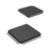
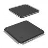
Package: 100-LQFP

Quality and Safety Features

Brown-out Detect/Reset for power stability

Industrial temperature range ensures operation in varied environments

Compatibility

Compatible with a range of development tools and software from STMicroelectronics

Flexible interfacing with various digital and analog devices

Application Areas

Industrial control systems

Medical instrumentation

Advanced IoT devices

Automotive applications

Consumer electronics

Product Lifecycle

Status: Active

Product is not nearing discontinuation, ongoing support and availability expected

Several Key Reasons to Choose This Product

Robust processing capabilities with the ARM Cortex-M3 core

Extensive memory and connectivity options accommodate demanding applications

Low power profile suits battery-powered devices

Comprehensive safety and quality features ensure product reliability

Backed by STMicroelectronics' extensive support and resources

Frequently Asked Questions(FAQ)

What are the key differences between the STM32F215VGT6 and other STM32F2 series microcontrollers in terms of memory configuration and peripheral integration for industrial automation applications?
The STM32F215VGT6 distinguishes itself within the STM32F2 family by offering a 1MB (1M x 8) embedded Flash memory and 132KB of RAM, providing sufficient code storage and data handling capacity for complex industrial control algorithms. Unlike lower-end F2 variants with reduced memory footprints, this model maintains full connectivity through CANbus, USB OTG, and dual 12-bit ADCs without sacrificing core performance at its 120MHz operating frequency. Its balanced architecture supports real-time processing requirements common in motor control and sensor fusion systems where deterministic execution is critical.
How does the STM32F215VGT6 handle power supply variations in battery-powered edge devices, and what design considerations should be made regarding its voltage regulator and brown-out detection features?
Operating across a 1.8V to 3.6V supply range, the STM32F215VGT6 enables flexible deployment in both low-power and high-performance battery applications such as IoT sensors or portable test equipment. The integrated brown-out reset (BOR) circuitry automatically monitors VDD and triggers a system reset if voltage drops below safe thresholds—typically programmable at several levels via software. This feature prevents erratic behavior during sudden load changes or transient dips, which is essential when using switching regulators or harvesting energy from unstable sources like solar cells.
Can the STM32F215VGT6 interface directly with legacy RS-485 networks while also supporting modern USB communication protocols, and how do these concurrent interfaces impact PCB layout complexity?
Yes, the STM32F215VGT6 includes UART/USART peripherals that can be configured for RS-485 mode using external transceivers, allowing seamless integration into industrial fieldbus environments. Simultaneously, its native USB OTG capability supports device or host modes for PC connectivity or power delivery. However, simultaneous use requires careful attention to ground plane segmentation, impedance matching on high-speed traces, and isolation between analog and digital sections to avoid cross-talk—especially when driving both differential serial lines and USB D+/D- signals from shared I/O pins.
What are the thermal implications of running the STM32F215VGT6 at maximum clock speed under continuous load, and how does package choice influence junction temperature management in compact enclosures?
At 120MHz with all peripherals active, the STM32F215VGT6 may dissipate up to 100–150 mW depending on activity factor and VDD. In the 100-LQFP (14x14) package, this results in a typical junction-to-ambient thermal resistance (θJA) of around 50°C/W, meaning temperatures could rise 5–7.5°C above ambient under worst-case conditions. For designs in sealed enclosures without airflow, consider adding thermal vias beneath the IC or selecting an exposed pad variant if available; otherwise, derating operation below peak frequencies becomes necessary to maintain reliability over time.
How does the internal oscillator of the STM32F215VGT6 compare to external crystal solutions in terms of timing accuracy and long-term stability for precision measurement systems?
While the internal 16 MHz HSI oscillator provides adequate timing for most general-purpose tasks, it typically exhibits ±1% initial accuracy and drifts with temperature and aging—unacceptable for applications requiring sub-microsecond synchronization across distributed nodes. In contrast, an external 8 MHz crystal with ±20 ppm stability offers far superior long-term precision, reducing cumulative timing errors in multi-sensor networks. The STM32F215VGT6 supports both options, but switching to external crystals necessitates additional PCB space, loading capacitors, and potential recalibration routines in firmware.
Is it feasible to use the STM32F215VGT6 for real-time image preprocessing given its lack of dedicated DSP instructions, and what architectural trade-offs must be evaluated?
Although lacking hardware DSP blocks found in some ARM Cortex-M4/M7 cores, the STM32F215VGT6’s 120MHz Cortex-M3 can still perform basic image operations such as edge detection or grayscale conversion using optimized C code or CMSIS-DSP library functions. However, frame rates will be limited compared to devices with single-cycle MAC units or SIMD support. For VGA-resolution processing at >10 fps, consider offloading to a companion sensor hub or upgrading to a higher-performance MCU—unless downsampling or leveraging DMA-based block transfers significantly reduces CPU overhead.
How does the number of available GPIO pins (82) in the STM32F215VGT6 affect expansion strategies when connecting multiple SPI sensors simultaneously?
With 82 user-accessible I/Os, the STM32F215VGT6 can independently address up to four SPI devices without multiplexing, assuming each uses one chip select line. However, shared buses (e.g., MISO/MOSI/SCLK) require software-controlled CS toggling, increasing latency. Careful assignment of CS pins to dedicated GPIOs avoids contention, while using alternate function remapping ensures optimal signal routing. Still, designers must account for pin reuse constraints during layout—particularly if LCD or Ethernet features are also enabled—potentially limiting simultaneous sensor operation.
What role does the DMA controller play in optimizing throughput for the STM32F215VGT6 when transferring ADC samples to memory without CPU intervention?
The STM32F215VGT6 integrates a 7-channel DMA controller capable of offloading data movement from the Cortex-M3 core. During ADC conversions, setting up a DMA stream allows automatic transfer of 16-sample sequences into SRAM buffers upon completion, eliminating interrupt service routine overhead. This enables sustained sampling at up to 3 MSPS per ADC channel (with proper buffer sizing), preserving CPU cycles for higher-level logic. Misconfiguration risks include buffer overflows or misaligned addresses, so double-buffering techniques are recommended for continuous acquisition scenarios.
How does the STM32F215VGT6 comply with automotive-grade reliability standards despite being classified as commercial temperature range (-40°C to +85°C), and what testing protocols apply during qualification?
While rated for industrial environments rather than AEC-Q100 Grade 1 (which covers -40°C to +125°C), the STM32F215VGT6 undergoes rigorous factory testing including ESD, latch-up immunity, and parametric validation per JEDEC standards. It supports extended temperature operation through controlled manufacturing processes and layout guidelines. Designers targeting automotive applications should supplement with conformal coating, robust PCB stack-up, and functional safety planning—even though the part itself isn’t certified for ASIL levels without additional system-level mitigations.
Can the STM32F215VGT6 drive a character LCD module directly, and what limitations arise from its PWM and GPIO capabilities?
Yes, the STM32F215VGT6 can interface with character LCDs via parallel output using general-purpose I/O pins or through SPI/I2C with external drivers. However, contrast control via PWM requires configuring one of the 16 advanced-control timers (TIM1/TIM8) or general-purpose PWM modules. Since only two 12-bit DACs exist (not usable for LCD bias), external op-amps or charge pumps may be needed for voltage scaling. Additionally, backlight dimming consumes significant current if LEDs are driven directly from 3.3V rails, necessitating MOSFET switches to prevent excessive power draw.
What precautions should be taken when programming the STM32F215VGT6 via SWD after production assembly to avoid accidental flash corruption?
To prevent unintended writes during debugging, disable write protection in Option Bytes before flashing—though many development boards auto-handle this. Post-programming, lock the device using RDP Level 1 to allow read access while blocking further modifications unless unlocked intentionally. Also verify that NRST pin isn’t inadvertently held low during power-up, as this prevents SWD communication entirely. Always confirm boot mode selection (BOOT0/BOOT1) matches expected flash start address after reset.
How does the Moisture Sensitivity Level (MSL) of 3 for the STM32F215VGT6 impact storage and handling in humid manufacturing environments?
Classified as MSL 3 (168-hour limit after opening bag), the STM32F215VGT6 must remain in a dry environment (<10% RH) post-delivery until soldering. Once unsealed, components should be baked if stored beyond 168 hours to remove absorbed moisture, preventing pop-corning during reflow. Standard lead-free solder profiles (~245°C peak) are acceptable, but exceeding 260°C for prolonged durations degrades bond integrity. Facilities without humidity-controlled packaging areas risk latent defects even if visual inspection appears normal.
What are the implications of using the STM32F215VGT6 in wireless mesh networks where nodes intermittently lose power, and how does its low-power modes compare to duty-cycled alternatives?
In battery-operated mesh topologies, the STM32F215VGT6’s Stop Mode reduces consumption to ~2 µA with RTC and SRAM retention—suitable for sleep intervals of minutes. However, wake-up latency (~2 µs) and context restoration overhead limit responsiveness compared to ultra-low-power MCUs with faster state transitions. If nodes transmit hourly bursts, this trade-off may be acceptable; otherwise, consider devices with deep sleep <1 µA or hardware-assisted wake-on-RF. Flash writes during active periods also incur erase/write cycles, so wear leveling is advised for logging applications.
How does the STM32F215VGT6 support secure firmware updates over-the-air (OTA) despite lacking cryptographic accelerators?
Without built-in AES/SHA engines, the STM32F215VGT6 relies on software-based cryptography libraries (e.g., mbed TLS ported to Cortex-M3). Implementing RSA-2048 or ECC-P256 signatures increases CPU load and flash usage, potentially halting update processes under heavy background tasks. Designers must balance security needs against real-time constraints, possibly restricting updates to maintenance windows or using symmetric keys with periodic rotation. Secure bootloaders should validate hashes against pre-stored roots before executing new images.
What factors determine whether the STM32F215VGT6 can reliably operate in electrically noisy environments such as switch-mode power supplies or motor drives?
Robustness against EMI depends on layout practices more than MCU specs alone. Keep analog inputs (especially ADC channels) away from switching nodes, use guard rings, and route sensitive traces perpendicular to high-current paths. The device’s 1.8–3.6V tolerance helps tolerate minor supply ripple, but sudden transients (>100 mV/ns) may corrupt registers without external TVS diodes. Decoupling capacitors near VDD/VSS pins and minimizing loop area in power traces reduce susceptibility. Always conduct pre-compliance tests with EFT burst generators during prototyping.
How does the absence of EEPROM in the STM32F215VGT6 affect non-volatile parameter storage strategies in calibration-heavy instrumentation?
Lacking internal EEPROM, the STM32F215VGT6 requires alternative approaches for storing trim values or user settings persistently. Options include reserving small blocks of Flash (with wear leveling), using FRAM via SPI, or caching in RAM with periodic backup to external NVRAM. Flash endurance (~10k cycles) limits frequent writes, so delta encoding or checksum validation minimizes erasures. External I²C EEPROMs like 24LC256 add cost and footprint but provide proven reliability for static data.
What considerations apply when cascading multiple STM32F215VGT6 devices in a multi-master I²C network for distributed sensing?
Supporting I²C at 400 kHz standard mode, the STM32F215VGT6 can participate in multi-master setups, but arbitration failures during contention require robust retry logic in firmware. Each node must have unique addresses, and pull-up resistors (typically 4.7 kΩ) must accommodate total bus capacitance from all devices plus PCB parasitics. Long cable runs (>1m) demand stronger pull-ups or repeaters. Clock stretching adds timing uncertainty, especially if slaves have variable processing delays—so timeout thresholds must exceed worst-case slave response times.
How does the STM32F215VGT6’s CANbus implementation handle message prioritization and error recovery in safety-critical automotive subsystems?
The integrated bxCAN controller follows ISO 11898-1 standards, supporting message filtering, priority-based arbitration, and automatic retransmission upon bus-off events. Each mailbox can be assigned to specific IDs, enabling deterministic latency for critical messages. Error counters monitor dominant/recessive bit mismatches, triggering passive or bus-off states if thresholds are exceeded. While not ASIL-certified out-of-the-box, the hardware provides foundations for fail-operational behavior when paired with watchdog timers and redundant communication paths in system design.

Parts with Similar Specifications

The three parts on the right have similar specifications to STMicroelectronics STM32F215VGT6

Product Attribute STM32F215ZGT6 STM32F215RGT6 STM32F215VGT7 STM32F215RET6
Part Number STM32F215ZGT6 STM32F215RGT6 STM32F215VGT7 STM32F215RET6
Manufacturer STMicroelectronics STMicroelectronics STMicroelectronics STMicroelectronics
Number of I/O - - - -
Core Processor - - - -
Voltage - Supply (Vcc/Vdd) - - - -
Data Converters - - - -
Oscillator Type - - - -
Supplier Device Package - 196-NFBGA (12x12) 16-PDIP 64-VQFN (9x9)
Operating Temperature - -40°C ~ 85°C 0°C ~ 70°C -40°C ~ 85°C
Program Memory Size - - - -
Program Memory Type - - - -
Core Size - - - -
Peripherals - - - -
Base Product Number - DAC34H84 MAX500 ADS62P42
EEPROM Size - - - -
Series - - - -
Package - Tape & Reel (TR) Tube Tape & Reel (TR)
Speed - - - -
RAM Size - - - -
Connectivity - - - -
Package / Case - 196-LFBGA 16-DIP (0.300', 7.62mm) 64-VFQFN Exposed Pad
Mounting Type - Surface Mount Through Hole Surface Mount

STM32F215VGT6 Datasheet PDF

Download STM32F215VGT6 pdf datasheets and STMicroelectronics documentation for STM32F215VGT6 - STMicroelectronics.

PCN Packaging
2.73KHz.pdf
PCN Assembly/Origin
2.73KHz.pdf
PCN Design/Specification
Mult Dev 03/Nov/2022.pdf Mult Dev Material Chgs 28/Feb/2023.pdf STM32F2yyy 16/Jul/2021.pdf
HTML Datasheet
STM32 F2 Series Brochure.pdf STM32F215xx, STM32F217xx.pdf

Customer Reviews

Evaluation: 10 Articles

  • Dani***alkerTech
    Jun 1, 2026

    Product works, but setup took more effort than expected. Once configured the MCU ran reliably, although documentation support felt older compared with newer platforms. Fine for maintenance projects.

  • Yuki***aka88
    May 26, 2026

    信号通信プロジェクトでこのRS-485トランシーバーを使用しました。設置は簡単で、長距離ケーブルでも通信は安定していました。消費電力も、以前使用していたものより低くなっています。

  • Stev***aker
    May 20, 2026

    Solid diode for power rectification. Works well in switching circuits.

  • Bran***Lewis
    May 11, 2026

    Compact FPGA with good performance. Suitable for basic signal processing tasks.

  • Oliv***arris
    May 7, 2026

    Reliable I/O expander. Works well in embedded control applications.

  • Jess***Jones
    Apr 17, 2026

    It offers good value for the price, and the specifications match the description. I’ve been using it for two days with no issues, and I’ll definitely buy it again if I need it in the future.

  • Mich***Smith
    Apr 17, 2026

    Shipping was on time, the component pins are neatly aligned, and I tested 10 of them with a multimeter—all readings were within the specified range. Highly recommended.

  • Aman***arris
    Apr 3, 2026

    It was great—the entire process, from placing the order to receiving the package, went very smoothly. The components were consistent, the price was fair, and I had a very pleasant shopping experience.

  • Mike***nch
    Apr 3, 2026

    Better than expected! The resistance and capacitance readings were spot-on, and it passed the test on the first try. The service was reliable, and the packaging was thoughtful—I highly recommend it.

  • Daic***K.
    Mar 23, 2026

    Very good. No issue after long time testing.

Write a Review

Your Email address will not be published.

Shipment

Delivery Time

In-stock items can be shipped within 24 hours. Some parts will be arranged for delivery within 1-2 days from the date all items arrive at our warehouse. And Allelco ships order once a day at about 17:00, except Sunday. Once the goods are shipped, the estimated delivery time depends on the shipping methods and Delivery destination. The table below shows are the logistic time for some common countries.

Delivery Cost

  1. Use your express account for shipment if you have one.
  2. Use our account for the shipment. Refer to the table below for the approximate charges.
(Different time frame / countries / package size has different price.)

Delivery Method

  1. Global Common Shipment by DHL / UPS / FedEx / TNT / EMS / SF we support.
  2. Others more shipping ways, please get in touch with your customer manager.

Common Countries Logistic Time Reference
Region Country Logistic Time(Day)
America United States 5
Brazil 7
Europe Germany 5
United Kingdom 4
Italy 5
Oceania Australia 6
New Zealand 5
Asia India 4
Japan 4
Middle East Israel 6
DHL & FedEx Shipment Charges Reference
Shipment charges(KG) Reference DHL(USD$)
0.00kg-1.00kg USD$30.00 - USD$60.00
1.00kg-2.00kg USD$40.00 - USD$80.00
2.00kg-3.00kg USD$50.00 - USD$100.00
Note:
The above table is for reference only. There may have some data bias for the uncontrollable factors.
Contact us if you have any questions.
  • QC (Quality Warranty)
  • Payment Support
  • Packaging
  • Certifications & Memberships

QC (Quality Warranty)

Allelco is committed to exceeding customer expectations through customer service excellence, order accuracy, and on-time delivery.
This is achieved through our commitment to the continual improvement of our processes, services, and products.


Strict quality inspection builds a solid foundation for electronic component quality.
  1. Visual inspection
  2. Performance testing and reliability verification
  3. Standardized full-process testing
  4. Precise control of every parameter
We eliminate defective components and ensure the stable operation of electronic devices through professional quality standards.

Payment Support

The payment method can be chosen from the methods shown below: Wire Transfer (T/T, Bank Transfer), Western Union, Credit card, PayPal.
  • HKBea
  • Paypal
  • MasterCard
  • Western-Union
  • VISA
Stable Delivery, Sincere Partnership — Your Faithful Supply Chain Partner
  • Efficient Supply Management
  • Cost-Saving Procurement
  • Fast Sourcing & Delivery
Contact us if you have any questions.

Packaging

Electrostatic Discharge Protection and Handling

All electrostatic-sensitive components are handled in accordance with electrostatic discharge control procedures. The products are hermetically sealed in anti-static safe packaging to prevent electrostatic damage. Appropriate labeling is also applied for identification and traceability. This ensures product integrity during storage, handling and transportation.


ESD

Certifications & Memberships

Third-party certified, strict quality control. Our certification
  • ISO 9001: 2015
  • ISO 13485: 2016
  • ISO 14001: 2015
  • ISO 28000: 2007
  • ISO 45001: 2018
  • GB/T 27922-2011
  • SMTA
  • IPC
  • ESD
  • PSMA
STM32F215VGT6 Image

STM32F215VGT6

STMicroelectronics
32D-STM32F215VGT6

Want a better price? Add to Cart and Submit RFQ now, we'll contact you immediately.

0 RFQ
Shopping cart (0 Items)
It is empty.
Compare List (0 Items)
It is empty.
Feedback

Your feedback matters! At Allelco, we value the user experience and strive to improve it constantly.
Please share your comments with us via our feedback form, and we'll respond promptly.
Thank you for choosing Allelco.

Subject
E-mail
Comments
Captcha
Drag or click to upload file
Upload File
types: .xls, .xlsx, .doc, .docx, .jpg, .png and .pdf.
Max file size: 10MB