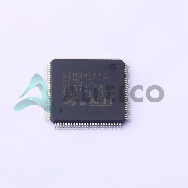
View All

Please refer to the English Version as our Official Version.Return

Europe
France(Français) Germany(Deutsch) Italy(Italia) Russian(русский) Poland(polski) Czech(Čeština) Luxembourg(Lëtzebuergesch) Netherlands(Nederland) Iceland(íslenska) Hungarian(Magyarország) Spain(español) Portugal(Português) Turkey(Türk dili) Bulgaria(Български език) Ukraine(Україна) Greece(Ελλάδα) Israel(עִבְרִית) Sweden(Svenska) Finland(Svenska) Finland(Suomi) Romania(românesc) Moldova(românesc) Slovakia(Slovenská) Denmark(Dansk) Slovenia(Slovenija) Slovenia(Hrvatska) Croatia(Hrvatska) Serbia(Hrvatska) Montenegro(Hrvatska) Bosnia and Herzegovina(Hrvatska) Lithuania(lietuvių) Spain(Português) Switzerland(Deutsch) United Kingdom(English)
Asia/Pacific
Japan(日本語) Korea(한국의) Thailand(ภาษาไทย) Malaysia(Melayu) Singapore(Melayu) Vietnam(Tiếng Việt) Philippines(Pilipino)
Africa, India and Middle East
United Arab Emirates(العربية) Iran(فارسی) Tajikistan(فارسی) India(हिंदी) Madagascar(malaɡasʲ)
South America / Oceania
New Zealand(Maori) Brazil(Português) Angola(Português) Mozambique(Português)
North America
United States(English) Canada(English) Haiti(Ayiti) Mexico(español)
HomeProductsIntegrated Circuits (ICs)Embedded - MicrocontrollersSTM32F446VCT6
STM32F446VCT6 Image
Image may be representation.
See specifications for product details.
EXPRESS OPTION
Payment method

STM32F446VCT6 - STMicroelectronics

Manufacturer Part Number
STM32F446VCT6
Manufacturer
STMicroelectronics
Allelco Part Number
32D-STM32F446VCT6
Warranty
1 Year Allelco Warranty - Find out more
Stock Status:
6,040 pcs available, New & Original
Parts Description
IC MCU 32BIT 256KB FLASH 100LQFP
Package
100-LQFP (14x14)
Data sheet
STM32F446VCT6.pdf

HTML Datasheet

STM32F446xC/E.pdf

PCN Packaging

2.73KHz.pdf

PCN Assembly/Origin

STM32 15/Nov/2019.pdf
RoHs Status
ROHS3 Compliant
Our certification
In stock: 6040
  • Unit Price: $5.056
  • Subtotal: $0.00

Want a better price?
Add to Cart and Submit RFQ now, we'll contact you immediately.

Quantity Unit Price Ext. Price
1+ $5.056 $5.06
10+ $4.255 $42.55
30+ $3.882 $116.46
100+ $3.571 $357.10
The above prices does not include taxes and freight rates, which will be calculated on the order pages.

Specifications

STM32F446VCT6 Tech Specifications
STMicroelectronics - STM32F446VCT6 technical specifications, attributes, parameters and parts with similar specifications to STMicroelectronics - STM32F446VCT6

Product Attribute Attribute Value
Manufacturer STMicroelectronics
Voltage - Supply (Vcc/Vdd) 1.7V ~ 3.6V
Supplier Device Package 100-LQFP (14x14)
Speed 180MHz
Series STM32F4
RAM Size 128K x 8
Program Memory Type FLASH
Program Memory Size 256KB (256K x 8)
Peripherals Brown-out Detect/Reset, DMA, I²S, LVD, POR, PWM, WDT
Package / Case 100-LQFP
Package Tray
Product Attribute Attribute Value
Oscillator Type Internal
Operating Temperature -40°C ~ 85°C (TA)
Number of I/O 81
Mounting Type Surface Mount
EEPROM Size -
Data Converters A/D 16x12b; D/A 2x12b
Core Size 32-Bit Single-Core
Core Processor ARM® Cortex®-M4
Connectivity CANbus, EBI/EMI, I²C, IrDA, LINbus, SAI, SD, SPDIF-Rx, SPI, UART/USART, USB, USB OTG
Base Product Number STM32F446

Environmental & Export Classifications

ATTRIBUTE DESCRIPTION
RoHs Status ROHS3 Compliant
Moisture Sensitivity Level (MSL) 3 (168 Hours)
REACH Status REACH Unaffected
ECCN 3A991A2
HTSUS 8542.31.0001

Parts Introduction

STM32F446VCT6 Image
STM32F446VCT6 (1)

Manufacturer Part Number

STM32F446VCT6

Manufacturer

STMicroelectronics

Introduction

High-performance ARM Cortex-M4 based microcontroller with advanced peripherals for real-time applications.

Product Features and Performance

Core Processor: ARM Cortex-M4

Speed: 180MHz

Program Memory Size: 256KB

RAM Size: 128KB

Analog-to-Digital Converter (ADC): 16 channels with 12-bit resolution

Digital-to-Analog Converter (DAC): 2 channels with 12-bit resolution

Number of I/O: 81

Advanced Connectivity: CANbus, I2C, USB, SPI, UART/USART, and more

Peripherals include DMA, PWM, Watchdog Timer, and Brown-out Detect

Internal Oscillator for device timing

Product Advantages

High processing power with 32-bit single-core ARM Cortex-M4

Efficient signal processing with DSP instructions

Extensive communication interface support for versatile use cases

Large set of embedded peripherals for complex applications

STM32F446VCT6 Image
STM32F446VCT6 (2)

Key Technical Parameters

Core Size: 32-Bit Single-Core

Voltage Supply: 1.7V to 3.6V

EBI/EMI, SAI, SD, SPDIF-Rx supported

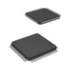
Surface Mount 100-LQFP Package for PCB assembly

Quality and Safety Features

Brown-out Detect/Reset for power safety

Low Voltage Detect (LVD) for battery applications

Temperature Range: -40°C to 85°C ensuring reliability in harsh conditions

Compatibility

Suited for applications requiring USB OTG

Compatible with CANbus systems

Supports multiple serial communication protocols

Application Areas

Industrial control systems

Consumer electronics

Automotive applications

Medical devices

Internet of Things (IoT)

Product Lifecycle

Status: Active (Not nearing discontinuation)

Manufacturer ensures availability of replacements and upgrades.

Several Key Reasons to Choose This Product

High-performance 180MHz ARM Cortex-M4 core for demanding applications

Extensive memory capabilities with 256KB Flash and 128KB RAM for complex programs

Broad connectivity options facilitate integration into various systems

Robust quality with safety features for critical applications

Active product support and long-term availability from STMicroelectronics

Frequently Asked Questions(FAQ)

How does the STM32F446VCT6 compare to other STM32F4 series microcontrollers in terms of program memory capacity and core processing speed, and what implications does this have for real-time control applications?
The STM32F446VCT6 offers 256KB of embedded Flash memory and operates at up to 180MHz using its ARM® Cortex®-M4 core with FPU. Within the STM32F4 family, this places it between lower-density variants like the STM32F407 (up to 192KB Flash) and higher-performance models such as the STM32F417 (up to 512KB). The 180MHz clock enables tight loop timing suitable for digital signal processing and motor control loops running at microsecond precision. However, designers must consider Flash wait states when operating near maximum frequency under full power, which may require careful layout and decoupling to maintain stability.
What are the key trade-offs involved when selecting the STM32F446VCT6 over an external microcontroller solution with separate Flash and SRAM chips, particularly regarding system reliability and development complexity?
Integrating 256KB of on-chip Flash and 128KB of SRAM eliminates the need for discrete memory components, reducing PCB footprint by approximately 15–20% compared to a discrete memory design. This integration also improves signal integrity by minimizing high-speed trace lengths. However, the fixed memory layout limits flexibility—larger codebases exceeding 256KB will require external NOR or PSRAM, adding cost and complexity. Additionally, while internal memory reduces component count and potential failure points, it also centralizes risk; a single ESD event or firmware corruption affects both program and data storage simultaneously.
In what scenarios would the USB OTG and SDIO peripherals of the STM32F446VCT6 be simultaneously utilized, and how should clocking and power sequencing be managed to avoid conflicts?
Simultaneous use of USB OTG and SDIO is common in portable data loggers or industrial gateways where a USB host port powers peripheral devices while reading sensor data via an SD card. The STM32F446VCT6 supports both interfaces through shared APB2 bus but requires independent PHYs. Clock accuracy is critical: USB mandates a 48MHz ±0.25% clock derived from the 12MHz HSE oscillator, while SDIO uses 48MHz for optimal throughput. Careful routing of these clocks and attention to VBUS sensing logic prevent contention during hot-plug events. Power sequencing must ensure VBUS stabilizes before enabling USB pull-ups to comply with USB 2.0 spec.
Can the STM32F446VCT6 drive multiple high-current loads directly from GPIO pins without additional buffering, and what are the recommended practices for protecting I/O lines during field upgrades?
No, GPIO pins on the STM32F446VCT6 can source or sink only up to 25mA continuously, with absolute maximum ratings of 20mA per pin and 125mA total for the entire port. Driving loads above these limits risks latch-up or permanent damage. For robust designs, external MOSFET drivers or level translators should be used. During field firmware updates, unpowered I/O lines can back-power the MCU if connected to active circuits. Implementing Schottky diodes on VDD lines or using bidirectional TVS arrays mitigates this risk. ST recommends keeping unused pins in analog mode with weak pull-downs to minimize leakage.
How does the operating voltage range of 1.7V to 3.6V influence battery-powered application design when using the STM32F446VCT6, and what impact does this have on wake-from-sleep performance?
The wide supply range allows operation from single-cell Li-ion batteries down to 1.7V, extending runtime in low-power modes. However, at voltages below 2.0V, the internal regulator begins to droop, potentially affecting PLL stability. In stop mode, the STM32F446VCT6 draws ~2µA, but transitioning back to run mode takes longer at lower voltages due to slower crystal startup times. Designers should verify that wake-up sequences complete within acceptable latency budgets when powered solely from a deeply discharged battery. Brown-out reset thresholds scale with Vdd, so brown-out detection must be configured conservatively for minimum Vdd.
What considerations apply when implementing CANbus communication with the STM32F446VCT6 in electrically noisy environments, and how does its CAN controller differ from basic UART implementations?
The STM32F446VCT6 includes a full-featured CAN 2.0B controller supporting baud rates up to 1Mbps. Unlike UART, CAN uses differential signaling (CANH/CANL), providing noise immunity through common-mode rejection. In harsh environments, termination resistors (120Ω) at both ends of the bus are essential, and twisted-pair cabling reduces EMI. The MCU’s built-in message filters reduce CPU load versus polling multiple UARTs. However, CAN arbitration introduces non-deterministic delays absent in UARTs, requiring real-time schedulers to manage message priorities correctly.
When interfacing the STM32F446VCT6 with a high-resolution ADC external to the chip, what precautions must be taken to avoid sampling errors caused by ground loops or reference instability?
Since the STM32F446VCT6 has only 16 internal 12-bit ADCs, external sensors often dictate the need for an off-chip ADC. Critical steps include ensuring star grounding between the MCU analog ground (AGND) and the external ADC’s analog ground, using separate traces back to the power plane to prevent digital switching currents from modulating the reference. A stable 2.048V reference (e.g., REF5025) is preferred over the internal bandgap. Sampling rates above 1MSPS may require careful layout to maintain ENOB > 10 bits. Decoupling capacitors near the ADC’s VREF pin should be placed within 5mm to suppress high-frequency transients.
How does the choice between using the internal RC oscillator versus an external crystal affect long-term system reliability in industrial deployments with the STM32F446VCT6?
The internal 16MHz RC oscillator (±1% accuracy) lacks thermal drift compensation, causing frequency variation across -40°C to 85°C that exceeds USB and CAN requirements. External crystals provide better stability (<±20ppm), essential for precise timing in Ethernet, USB, and motor control. While the internal oscillator simplifies BOM and reduces board space, it increases calibration overhead and risks compliance failures. Industrial systems typically mandate HSE/HSI trimming via factory calibration or software compensation. For applications requiring <0.1% timing accuracy, an 8–26MHz crystal with load capacitors matching the specified CL is strongly advised.
What role does the DMA engine play in optimizing performance when using the STM32F446VCT6 for continuous data acquisition via SPI or SAI interfaces, and how many channels can be active simultaneously?
The STM32F446VCT6 features a seven-channel DMA controller capable of offloading data transfers between peripherals and memory without CPU intervention. For SPI-based ADC readout, DMA can sustain 180MHz transfers at 22.5MB/s, effectively doubling throughput compared to interrupt-driven methods. The SAI interface supports TDM mode for multi-channel audio, where DMA handles frame synchronization. Up to four DMA streams can operate concurrently, but each stream shares two priority levels with other peripherals. Careful arbitration ensures low-latency responses for time-critical tasks like motor encoders or safety interlocks.
Are there known limitations when booting from user Flash versus system memory using the STM32F446VCT6, particularly regarding interrupt vector relocation and RAM usage?
Yes. Boot from system memory (address 0x1FFF0000) loads ST’s ROM-based bootloader, enabling serial download but disables user Flash programming until bootloader execution completes. This approach saves RAM but restricts firmware customization. Booting from main Flash allows full access to all peripherals but requires a valid IVT at address 0x08000000. If relocating the vector table to RAM (via SCB->VTOR), developers must ensure the first entry points to a valid stack pointer and second to Reset_Handler. Misconfiguration leads to HardFault. Also, Flash read-while-write operations consume extra cycles, impacting real-time performance during self-programming.
What are the thermal implications of running the STM32F446VCT6 at sustained 180MHz output in compact enclosures, and how does package choice influence junction temperature rise?
At 180MHz with all peripherals active, typical power dissipation reaches 80–100mW, resulting in a junction-to-ambient thermal resistance (θJA) of ~45°C/W in air. In sealed enclosures, ambient temperature rises, pushing TJ toward 85°C limit. The 100-LQFP package offers moderate thermal performance; switching to QFN with exposed pad reduces θJA by 30%. Without heatsinking, continuous operation near max frequency may trigger thermal shutdown. Monitoring Vdd droop during stress testing reveals internal current draw. Designers should derate clock speed in high-ambient conditions or add ventilation to maintain MTBF above 100,000 hours.
How does the presence of dual 12-bit DACs in the STM32F446VCT6 benefit mixed-signal applications, and what calibration procedures are required for precision output?
The integrated dual 12-bit DACs support simultaneous analog outputs for applications like PWM filtering or waveform generation, eliminating external DACs and saving board space. Each DAC shares a single reference input, requiring careful routing to avoid crosstalk. Output settling time is ~1.5µs for 1LSB accuracy. Calibration involves writing to DAC_DHRx registers after reset to compensate for offset and gain errors. ST provides factory-trimmed values in the device’s unique ID registers, but users may perform in-system calibration by measuring outputs with a precision ADC and adjusting DACCALR register accordingly. Noise performance degrades above 10kHz update rates due to internal switching.
When integrating the STM32F446VCT6 into a safety-critical system, what additional measures beyond datasheet recommendations are necessary to meet functional safety standards like ISO 13849?
While the STM32F446VCT6 is not certified for functional safety, designers can implement software redundancy, periodic self-tests (RAM parity check, CRC of critical variables), and watchdog monitoring to elevate reliability. Memory protection units (MPUs) isolate safety-critical tasks from application code. Dual-bank Flash allows rollback on corrupted firmware. However, achieving Cat. 3 PLd requires third-party certification, which demands hardware modifications such as redundant power supplies or error-correcting code (ECC) memory. Using this MCU in safety systems necessitates rigorous fault injection testing and documentation per IEC 61508 guidelines.
What are the implications of using the SPDIF-RX peripheral with the STM32F446VCT6 in consumer audio equipment, and how does it interact with the SAI interface?
SPDIF-RX decodes optical or coaxial digital audio streams into PCM data, useful in AV receivers or set-top boxes. It interfaces directly with the SAI block, bypassing CPU overhead. The STM32F446VCT6 supports SPDIF reception up to 192kHz/24-bit, but requires an external SPDIF receiver IC (e.g., TI TPD1E10B06) due to lack of internal physical layer. Timing alignment between SPDIF clock recovery and SAI sample rate converters must be managed via FIFO resynchronization registers. Mismatched buffer sizes cause audio dropouts. Power consumption spikes during active decoding, so disabling unused audio peripherals during standby improves battery life.
How does the Moisture Sensitivity Level (MSL) of 3 for the STM32F446VCT6 affect assembly house handling procedures, and what reflow profile deviations could compromise solder joint reliability?
MSL 3 indicates the part can withstand up to 168 hours of exposure to ambient humidity before requiring baking. Assembly facilities must track floor-life using barcodes or lot numbers. After 168 hours, baking at 125°C for 24 hours prevents popcorning during reflow. Standard JEDEC J-STD-020 profiles apply, but peak temperatures above 245°C or dwell times exceeding 30 seconds accelerate intermetallic growth in joints. The 100-LQFP’s fine pitch (0.5mm) exacerbates void formation if solder paste volume is inconsistent. X-ray inspection post-reflow catches most defects, but visual checks remain essential for corner joints.
What strategies mitigate electromagnetic interference (EMI) when routing signals near the STM32F446VCT6’s high-speed interfaces like USB or SAI in production PCBs?
High-speed signals demand controlled impedance traces (90Ω differential for USB, 100Ω for LVDS-like SAI). Stubs and vias introduce reflections; thus, keep trace lengths matched and minimize discontinuities. Place decoupling caps within 2mm of Vdd pins, using 0.1µF ceramic in parallel with 1µF tantalum for bulk filtering. Split power planes under the MCU to contain return currents, and avoid routing sensitive analog traces adjacent to digital nets. Adding guard rings around crystal oscillators reduces radiated emissions. ST’s AN4857 application note provides layout templates validated through CISPR 32 testing.
Why might a designer choose the STM32F446VCT6 over a Cortex-M7 variant despite similar core architecture, and what cost-performance trade-offs emerge?
The STM32F446VCT6 trades raw floating-point performance (single-precision only) and cache-less design against the STM32F7 or STM32H7 for DSP-heavy tasks. However, it offers better power efficiency at 180MHz (100mW vs. 300mW+) and lower unit cost ($8.50 in 1k quantities). Its rich peripheral mix—including dual DACs, SAI, and CAN—makes it ideal for embedded control without needing M7’s 480MHz capability. For applications with moderate compute needs (<50 DMIPS), the F446 provides sufficient headroom while simplifying thermal management and lowering BOM cost by 15–20%.

Parts with Similar Specifications

The three parts on the right have similar specifications to STMicroelectronics STM32F446VCT6

Product Attribute STM32F446VET6TR STM32F446VET6 STM32F446RCT6 STM32F446VCT7
Part Number STM32F446VET6TR STM32F446VET6 STM32F446RCT6 STM32F446VCT7
Manufacturer STMicroelectronics STMicroelectronics STMicroelectronics STMicroelectronics
Operating Temperature - -40°C ~ 85°C 0°C ~ 70°C -40°C ~ 85°C
Oscillator Type - - - -
Number of I/O - - - -
Speed - - - -
Core Processor - - - -
Supplier Device Package - 196-NFBGA (12x12) 16-PDIP 64-VQFN (9x9)
Voltage - Supply (Vcc/Vdd) - - - -
Package - Tape & Reel (TR) Tube Tape & Reel (TR)
Mounting Type - Surface Mount Through Hole Surface Mount
Core Size - - - -
Program Memory Type - - - -
Data Converters - - - -
Package / Case - 196-LFBGA 16-DIP (0.300', 7.62mm) 64-VFQFN Exposed Pad
Peripherals - - - -
EEPROM Size - - - -
Series - - - -
Program Memory Size - - - -
RAM Size - - - -
Connectivity - - - -
Base Product Number - DAC34H84 MAX500 ADS62P42

STM32F446VCT6 Datasheet PDF

Download STM32F446VCT6 pdf datasheets and STMicroelectronics documentation for STM32F446VCT6 - STMicroelectronics.

HTML Datasheet
STM32F446xC/E.pdf
PCN Packaging
2.73KHz.pdf
PCN Design/Specification
Mult Dev 03/Nov/2022.pdf Mult Dev Material Chgs 28/Feb/2023.pdf
PCN Assembly/Origin
STM32 15/Nov/2019.pdf

Customer Reviews

Evaluation: 10 Articles

  • Emil***rperTech
    Jun 23, 2026

    Works exactly as described. I used it as a USB-to-SPI bridge in a small MCU development project and communication was stable from the first setup.

  • Liam***terTech
    Jun 15, 2026

    Used this CPLD in a logic control project. Programming was straightforward and signal timing matched the design requirements.

  • Nath***rooks
    Jun 11, 2026

    Installed this power component in a converter board. Output remained stable under different load conditions and thermal performance was better than expected.

  • Dani***alkerTech
    Jun 1, 2026

    Product works, but setup took more effort than expected. Once configured the MCU ran reliably, although documentation support felt older compared with newer platforms. Fine for maintenance projects.

  • Yuki***aka88
    May 26, 2026

    信号通信プロジェクトでこのRS-485トランシーバーを使用しました。設置は簡単で、長距離ケーブルでも通信は安定していました。消費電力も、以前使用していたものより低くなっています。

  • Stev***aker
    May 20, 2026

    Solid diode for power rectification. Works well in switching circuits.

  • Bran***Lewis
    May 11, 2026

    Compact FPGA with good performance. Suitable for basic signal processing tasks.

  • Oliv***arris
    May 7, 2026

    Reliable I/O expander. Works well in embedded control applications.

  • Jess***Jones
    Apr 17, 2026

    It offers good value for the price, and the specifications match the description. I’ve been using it for two days with no issues, and I’ll definitely buy it again if I need it in the future.

  • Mich***Smith
    Apr 17, 2026

    Shipping was on time, the component pins are neatly aligned, and I tested 10 of them with a multimeter—all readings were within the specified range. Highly recommended.

Write a Review

Your Email address will not be published.

Shipment

Delivery Time

In-stock items can be shipped within 24 hours. Some parts will be arranged for delivery within 1-2 days from the date all items arrive at our warehouse. And Allelco ships order once a day at about 17:00, except Sunday. Once the goods are shipped, the estimated delivery time depends on the shipping methods and Delivery destination. The table below shows are the logistic time for some common countries.

Delivery Cost

  1. Use your express account for shipment if you have one.
  2. Use our account for the shipment. Refer to the table below for the approximate charges.
(Different time frame / countries / package size has different price.)

Delivery Method

  1. Global Common Shipment by DHL / UPS / FedEx / TNT / EMS / SF we support.
  2. Others more shipping ways, please get in touch with your customer manager.

Common Countries Logistic Time Reference
Region Country Logistic Time(Day)
America United States 5
Brazil 7
Europe Germany 5
United Kingdom 4
Italy 5
Oceania Australia 6
New Zealand 5
Asia India 4
Japan 4
Middle East Israel 6
DHL & FedEx Shipment Charges Reference
Shipment charges(KG) Reference DHL(USD$)
0.00kg-1.00kg USD$30.00 - USD$60.00
1.00kg-2.00kg USD$40.00 - USD$80.00
2.00kg-3.00kg USD$50.00 - USD$100.00
Note:
The above table is for reference only. There may have some data bias for the uncontrollable factors.
Contact us if you have any questions.
  • QC (Quality Warranty)
  • Payment Support
  • Packaging
  • Certifications & Memberships

QC (Quality Warranty)

Allelco is committed to exceeding customer expectations through customer service excellence, order accuracy, and on-time delivery.
This is achieved through our commitment to the continual improvement of our processes, services, and products.


Strict quality inspection builds a solid foundation for electronic component quality.
  1. Visual inspection
  2. Performance testing and reliability verification
  3. Standardized full-process testing
  4. Precise control of every parameter
We eliminate defective components and ensure the stable operation of electronic devices through professional quality standards.

Payment Support

The payment method can be chosen from the methods shown below: Wire Transfer (T/T, Bank Transfer), Western Union, Credit card, PayPal.
  • HKBea
  • Paypal
  • MasterCard
  • Western-Union
  • VISA
Stable Delivery, Sincere Partnership — Your Faithful Supply Chain Partner
  • Efficient Supply Management
  • Cost-Saving Procurement
  • Fast Sourcing & Delivery
Contact us if you have any questions.

Packaging

Electrostatic Discharge Protection and Handling

All electrostatic-sensitive components are handled in accordance with electrostatic discharge control procedures. The products are hermetically sealed in anti-static safe packaging to prevent electrostatic damage. Appropriate labeling is also applied for identification and traceability. This ensures product integrity during storage, handling and transportation.


ESD

Certifications & Memberships

Third-party certified, strict quality control. Our certification
  • ISO 9001: 2015
  • ISO 13485: 2016
  • ISO 14001: 2015
  • ISO 28000: 2007
  • ISO 45001: 2018
  • GB/T 27922-2011
  • SMTA
  • IPC
  • ESD
  • PSMA
STM32F446VCT6 Image

STM32F446VCT6

STMicroelectronics
32D-STM32F446VCT6

Want a better price? Add to Cart and Submit RFQ now, we'll contact you immediately.

0 RFQ
Shopping cart (0 Items)
It is empty.
Compare List (0 Items)
It is empty.
Feedback

Your feedback matters! At Allelco, we value the user experience and strive to improve it constantly.
Please share your comments with us via our feedback form, and we'll respond promptly.
Thank you for choosing Allelco.

Subject
E-mail
Comments
Captcha
Drag or click to upload file
Upload File
types: .xls, .xlsx, .doc, .docx, .jpg, .png and .pdf.
Max file size: 10MB