
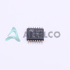

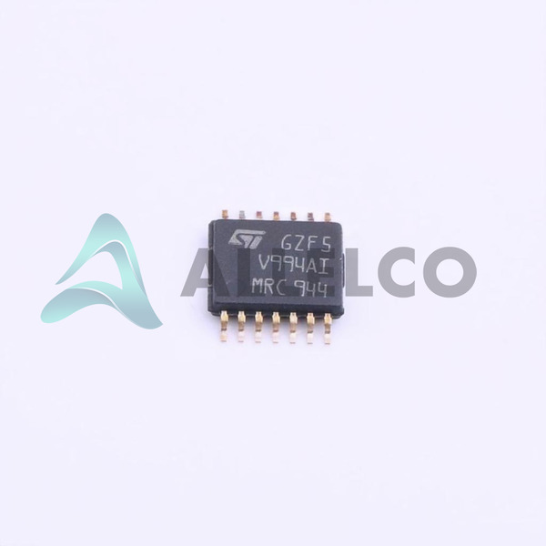
TSV994AIPT (1)
Manufacturer Part Number
TSV994AIPT
Manufacturer
STMicroelectronics
Introduction
Quad Operational Amplifier
Designed for general-purpose applications
Product Features and Performance
Rail-to-Rail Output
20 MHz Gain Bandwidth Product
10 V/μs Slew Rate
100 μV Input Offset Voltage
1 pA Input Bias Current
35 mA Output Current per Channel
820 μA Supply Current per Amplifier
Product Advantages
Suitable for a wide range of applications
Excellent performance characteristics
Low power consumption
Compact 14-TSSOP package
TSV994AIPT (2)
Key Technical Parameters
Supply Voltage Range: 2.5 V to 5.5 V
Operating Temperature Range: -40°C to 125°C
Package: 14-TSSOP
Quality and Safety Features
RoHS3 Compliant
AEC-Q100 Qualified (Automotive Grade)
Compatibility
Compatible with a variety of electronic systems and circuits
Application Areas
Automotive electronics
Industrial control systems
Portable and battery-powered devices
Instrumentation and measurement equipment
Product Lifecycle
Current product, not nearing discontinuation
Replacement and upgrade options available
Key Reasons to Choose This Product
Excellent performance and reliability
Wide operating temperature range
Low power consumption
Compact and space-efficient package
Automotive and industrial grade quality
 TSV992IYSTSTMicroelectronicsIC OPAMP GP 2 CIRCUIT 8MINISO
 TSV992IDTSTMicroelectronicsIC OPAMP GP 2 CIRCUIT 8SOIC
 TSVD-HCQ33S-122.880MTransko Electronics, Inc.XTAL OSC XO 122.8800MHZ CMOS SMD
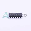 TSV994IDTSTMicroelectronicsIC OPAMP GP 4 CIRCUIT 14SO
 TSV992IQ2TSTMicroelectronics
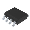 TSV992IDSTMicroelectronicsIC OPAMP GP 2 CIRCUIT 8SOIC
 TSV994STMicroelectronics


