View All

Please refer to the English Version as our Official Version.Return

Europe
France(Français) Germany(Deutsch) Italy(Italia) Russian(русский) Poland(polski) Czech(Čeština) Luxembourg(Lëtzebuergesch) Netherlands(Nederland) Iceland(íslenska) Hungarian(Magyarország) Spain(español) Portugal(Português) Turkey(Türk dili) Bulgaria(Български език) Ukraine(Україна) Greece(Ελλάδα) Israel(עִבְרִית) Sweden(Svenska) Finland(Svenska) Finland(Suomi) Romania(românesc) Moldova(românesc) Slovakia(Slovenská) Denmark(Dansk) Slovenia(Slovenija) Slovenia(Hrvatska) Croatia(Hrvatska) Serbia(Hrvatska) Montenegro(Hrvatska) Bosnia and Herzegovina(Hrvatska) Lithuania(lietuvių) Spain(Português) Switzerland(Deutsch) United Kingdom(English)
Asia/Pacific
Japan(日本語) Korea(한국의) Thailand(ภาษาไทย) Malaysia(Melayu) Singapore(Melayu) Vietnam(Tiếng Việt) Philippines(Pilipino)
Africa, India and Middle East
United Arab Emirates(العربية) Iran(فارسی) Tajikistan(فارسی) India(हिंदी) Madagascar(malaɡasʲ)
South America / Oceania
New Zealand(Maori) Brazil(Português) Angola(Português) Mozambique(Português)
North America
United States(English) Canada(English) Haiti(Ayiti) Mexico(español)
HomeProductsDiscrete Semiconductor ProductsDiodes - Bridge RectifiersDF10SA-E3/77
DF10SA-E3/77 Image
Image may be representation.
See specifications for product details.
EXPRESS OPTION
Payment method

DF10SA-E3/77 - Vishay General Semiconductor - Diodes Division

Manufacturer Part Number
DF10SA-E3/77
Manufacturer
Vishay General Semiconductor – Diodes Division
Allelco Part Number
32D-DF10SA-E3/77
Warranty
1 Year Allelco Warranty - Find out more
Stock Status:
128,010 pcs available, New & Original
Parts Description
BRIDGE RECT 1PHASE 1KV 1A DFS
Package
DFS
Data sheet
DF10SA-E3/77.pdf

PCN Design/Specification

DD-015-2015-Rev-0 07/Apr/2015.pdf

HTML Datasheet

DF005SA thru DF10SA.pdf

PCN Assembly/Origin

Multipe Parts 06/Sep/2022.pdf

Other Related Documents

Packaging Information.pdf
RoHs Status
ROHS3 Compliant
Our certification
In stock: 128010
  • Unit Price: $0.323
  • Subtotal: $0.00

Want a better price?
Add to Cart and Submit RFQ now, we'll contact you immediately.

Quantity Unit Price Ext. Price
1+ $0.323 $0.32
10+ $0.264 $2.64
30+ $0.238 $7.14
100+ $0.205 $20.50
500+ $0.192 $96.00
1500+ $0.182 $273.00
The above prices does not include taxes and freight rates, which will be calculated on the order pages.

Specifications

DF10SA-E3/77 Tech Specifications
Vishay General Semiconductor - Diodes Division - DF10SA-E3/77 technical specifications, attributes, parameters and parts with similar specifications to Vishay General Semiconductor - Diodes Division - DF10SA-E3/77

Product Attribute Attribute Value
Manufacturer Vishay General Semiconductor – Diodes Division
Voltage - Peak Reverse (Max) 1 kV
Voltage - Forward (Vf) (Max) @ If 1.1 V @ 1 A
Technology Standard
Supplier Device Package DFS
Series -
Package / Case 4-SMD, Gull Wing
Product Attribute Attribute Value
Package Tape & Reel (TR)
Operating Temperature -55°C ~ 150°C (TJ)
Mounting Type Surface Mount
Diode Type Single Phase
Current - Reverse Leakage @ Vr 5 µA @ 1000 V
Current - Average Rectified (Io) 1 A
Base Product Number DF10

Environmental & Export Classifications

ATTRIBUTE DESCRIPTION
RoHs Status ROHS3 Compliant
Moisture Sensitivity Level (MSL) 1 (Unlimited)
REACH Status REACH Unaffected
ECCN EAR99
HTSUS 8541.10.0080

Parts Introduction

DF10SA-E3/77 Image
DF10SA-E3/77 (1)

Manufacturer Part Number

DF10SA-E3/77

Manufacturer

Vishay

Introduction

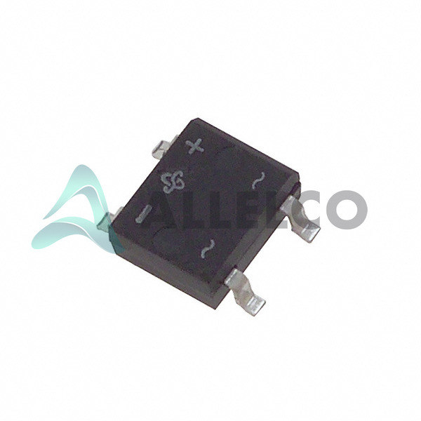
The DF10SA-E3/77 is a single-phase bridge rectifier from Vishay's semiconductor diode product line.

Product Features and Performance

Standard technology single-phase bridge rectifier

Surface Mount package for easier PCB integration

High maximum operating temperature range

Low forward voltage drop

Designed for high efficiency in rectification

Product Advantages

Optimal performance in compact 4-SMD, Gull Wing package

Low leakage current enhances energy efficiency

High reverse voltage capability suitable for a variety of applications

Robust temperature performance for operation in extreme conditions

Key Technical Parameters

Diode Type: Single Phase

Voltage - Peak Reverse (Max): 1 kV

Current - Average Rectified (Io): 1 A

Voltage - Forward (Vf) (Max) @ If: 1.1 V @ 1 A

Current - Reverse Leakage @ Vr: 5 µA @ 1000 V

Operating Temperature: -55°C ~ 150°C (TJ)

Quality and Safety Features

Compliance with industry standards for safety and performance

High temperature tolerance ensuring reliability under stress

Compatibility

Compatible with surface mount technology for PCB assembly

Suitable for various single-phase rectification applications

Application Areas

Power supplies

Consumer electronics

Industrial equipment

Communications infrastructure

Product Lifecycle

Active product status, not nearing discontinuation

Availability of replacements or upgrades not specified

Several Key Reasons to Choose This Product

Highly reliable surface mount bridge rectifier from a reputable manufacturer

Capable of withstanding high temperatures, making it suitable for tough environments

Low power loss due to reduced forward voltage and leakage current

1 kV reverse voltage rating enables usage in higher voltage circuits

Tape & Reel packaging suitable for automated assembly processes

Frequently Asked Questions(FAQ)

How does the DF10SA-E3/77 bridge rectifier compare to other single-phase surface-mount diodes in terms of reverse leakage current and peak voltage handling, and what design implications should engineers consider when selecting it for high-voltage power supply circuits?
The DF10SA-E3/77 exhibits a reverse leakage current of 5 µA at 1000 V, which is relatively low for its 1 kV peak reverse voltage rating and supports stable performance in high-voltage, low-current applications such as switch-mode power supplies or DC-DC converters. When compared to standard silicon bridge rectifiers with similar ratings, this leakage level reduces thermal drift and improves efficiency under partial-load conditions. However, in precision analog front-ends or low-power sensor interfaces, even this small leakage may necessitate careful PCB layout to avoid coupling noise through parasitic paths. Its 1 A average rectified current and 1.1 V forward voltage drop place it between general-purpose and high-efficiency rectifiers—making it suitable where moderate power levels and robust insulation are required, but not ideal for ultra-low-loss systems where Schottky alternatives might be preferred despite their lower voltage limits.
What are the key differences between the DF10SA-E3/77 and alternative bridge rectifiers like the KBPC series or WOG series when used in industrial motor drive applications, particularly regarding thermal performance and reliability under sustained load?
While the DF10SA-E3/77 operates reliably up to 150°C junction temperature, its DFS package (4-SMD gull wing) has limited heat dissipation compared to through-hole or larger molded packages like those used in KBPC or WOG series. In continuous-duty motor drives running near full load, the DF10SA-E3/77 may require derating due to reduced airflow over the small surface area. Additionally, its 1 kV isolation rating aligns well with industrial standards, but users must ensure creepage distances meet safety regulations. Unlike higher-power bridge modules designed for heatsinking, the DF10SA-E3/77 is better suited for intermittent or controlled environments where thermal mass or conduction paths can manage transient loads without exceeding TJ limits.
Can the DF10SA-E3/77 be safely used in automotive lighting systems operating at 12 V or 24 V DC, considering its voltage and current specifications, and what additional considerations apply beyond basic datasheet compliance?
Although the DF10SA-E3/77 exceeds nominal system voltages with its 1 kV reverse rating, it lacks the specific automotive-grade qualification (e.g., AEC-Q101) and environmental robustness required for direct use in harsh automotive environments. While it could technically function in non-critical auxiliary circuits with proper filtering, exposure to vibrations, humidity, and thermal cycling may compromise solder joints in its SMD configuration. Engineers should instead select components explicitly rated for automotive operation, even if over-engineered, to ensure longevity. The DF10SA-E3/77 remains viable only in non-automotive or controlled industrial settings where environmental stress is minimized.
Why would an engineer choose the DF10SA-E3/77 over discrete diode solutions when designing a compact AC-to-DC converter, and how does its integration affect board real estate and EMI characteristics?
The DF10SA-E3/77 integrates four diodes into a single monolithic package, reducing component count, minimizing parasitic inductance and capacitance compared to discrete implementations, and improving symmetry in bridge configurations. This contributes to more predictable switching behavior and lower radiated emissions—important for meeting CISPR standards. Its small 4-SMD footprint saves significant board space versus discrete alternatives, enabling compact designs. However, the shared internal layout means failure of one diode affects all four, increasing functional risk. For high-reliability applications, redundancy or post-manufacturing testing may be necessary. Still, for cost-sensitive, space-constrained designs where moderate power levels suffice, the DF10SA-E3/77 offers a practical balance of integration and performance.
What impact does the MSL 1 classification have on the DF10SA-E3/77 during reflow soldering, and how should assembly processes be managed to maintain long-term reliability?
With a Moisture Sensitivity Level (MSL) of 1, the DF10SA-E3/77 is exempt from moisture pre-conditioning and can be stored indefinitely without special handling before reflow. This simplifies inventory management and accelerates production workflows. During assembly, standard lead-free reflow profiles (typically peak temperatures around 245–260°C) are acceptable provided dwell times above melting point remain within JEDEC guidelines. However, excessive thermal exposure can degrade bond wires or die adhesion inside the DFS package. Manufacturers should validate their specific oven profiles against Vishay’s recommended conditions to avoid latent defects that manifest later in field operation.
How does the forward voltage drop of 1.1 V at 1 A influence efficiency in low-input-voltage power supplies using the DF10SA-E3/77, and what trade-offs exist versus alternative rectification strategies?
At 1 A, the DF10SA-E3/77 dissipates approximately 1.1 W per diode leg, totaling ~4.4 W in a full bridge—significant in low-voltage systems where input energy is already marginal. For example, in a 9 V input buck converter, this loss reduces available output power by nearly 10%. Engineers might consider synchronous rectification or active PFC stages to offset losses, but these add complexity. Alternatively, using lower-Vf Schottkys is not feasible due to their voltage limitations. Thus, the DF10SA-E3/77 is best applied where input voltages exceed 15–20 V, or where the benefits of integrated isolation outweigh conduction penalties.
What role does the DFS package play in the electrical and mechanical performance of the DF10SA-E3/77, and why might designers prefer it over SOIC-based bridge rectifiers?
The DFS (Dual Flat No-Lead Surface Mount) package provides excellent electrical conductivity via copper lead frames, supports high-frequency operation due to short leads, and enables automated pick-and-place assembly. Its gull-wing terminals enhance solder fillet strength compared to flat leads, improving mechanical resilience during thermal cycling. Unlike SOIC packages, DFS avoids plastic mold compound issues and offers superior thermal impedance through exposed pads when properly soldered. For the DF10SA-E3/77, this results in reliable operation across -55°C to +150°C, making it preferable in ruggedized or space-constrained applications where both durability and manufacturability are critical.
In what scenarios would the DF10SA-E3/77 be unsuitable despite meeting nominal voltage and current requirements, and how can system-level analysis help identify such cases early?
Even though the DF10SA-E3/77 meets basic specs, it becomes unsuitable in high-switching-frequency applications (>100 kHz) due to inherent reverse recovery charge (Qrr) typical of silicon PN junctions, leading to increased switching losses and potential thermal runaway. Similarly, in pulsed-load environments with rapid duty cycles, cumulative heating may push junction temperatures beyond safe limits despite average current being below 1 A. System modeling using Spice models or thermal simulations helps anticipate these effects. Designers should evaluate not just steady-state parameters but also transient response, switching harmonics, and ambient cooling—factors not always evident from static datasheet values alone.
How does RoHS3 compliance and REACH unaffected status influence global market deployment of products containing the DF10SA-E3/77, and what documentation should be retained during supply chain audits?
RoHS3 compliance ensures the DF10SA-E3/77 meets EU directives restricting hazardous substances like lead, mercury, and cadmium, facilitating entry into European markets without additional testing. REACH unaffected status indicates no SVHCs (Substances of Very High Concern) above threshold concentrations, reducing registration burdens under ECHA regulations. During audits, suppliers should provide certificates of conformance, material composition reports, and conflict mineral statements. Retaining batch-specific traceability data is essential for recalls or regulatory inquiries, especially in defense, medical, or aerospace sectors where supply chain integrity is mandated.
What precautions are necessary when paralleling multiple DF10SA-E3/77 units to increase current capacity, and how do manufacturing tolerances affect current sharing accuracy?
Paralleling the DF10SA-E3/77 requires careful attention to Vf mismatch—typical ±0.1 V variation across batches—which causes uneven current distribution under load. Without ballast resistors or active balancing, one unit may carry disproportionate current, accelerating aging or causing premature failure. Thermal coupling helps somewhat due to shared PCB plane, but initial mismatches persist. Best practice involves selecting devices from the same lot, limiting parallel counts to two or three, and incorporating current-sense feedback if high reliability is needed. Alternatively, using a single higher-current bridge rectifier may offer better consistency than risk-prone parallel arrangements.
How does the base product number DF10 relate to other variants like DF10S or DF10SMF, and what factors should guide selection among them for a given application?
The DF10 base covers a family of bridge rectifiers differentiated by packaging (e.g., SMD vs. through-hole), mounting style, and sometimes performance bins. The DF10SA-E3/77 uses a surface-mount DFS package with specific orientation marking. Other variants like DF10SMF may offer similar ratings but with different thermal profiles or pinouts. Selection hinges on mechanical constraints, thermal management strategy, and assembly method rather than electrical differences. Engineers should consult full variant matrices in manufacturer literature to confirm interchangeability—especially regarding polarity markings and pad layouts—to avoid costly redesigns during production handoffs.
What are the implications of the ECCN EAR99 classification for international sourcing of the DF10SA-E3/77, and how does this affect export controls in defense or satellite projects?
ECCN EAR99 designates the DF10SA-E3/77 as a "commodity" under U.S. Export Administration Regulations, meaning it generally falls outside strict licensing requirements unless incorporated into restricted end-products. However, exporters must still comply with general prohibitions (e.g., military end-use restrictions). In defense or satellite applications, even commodity components require thorough supply chain vetting to prevent diversion. Documentation should include end-user certificates and technical justification for component choice. While not inherently controlled, misuse risks necessitate due diligence regardless of ECCN status, particularly when working with foreign foundries or distributors lacking clear provenance trails.
How does the absence of a dedicated snubber circuit recommendation in the DF10SA-E3/77 datasheet reflect its intended use case, and what design practices mitigate inductive kickback risks in real-world installations?
The lack of explicit snubber guidance suggests the DF10SA-E3/77 is expected to operate in resistive or moderately inductive loads without extreme dv/dt stresses. However, in motor drives or transformer secondary sides, inductive transients can induce voltage spikes exceeding 1 kV, potentially damaging internal bonds. Mitigation includes proper grounding, twisted-pair wiring, and proximity to surge suppressors. If switching occurs rapidly, adding RC networks across each diode pair (not just the bridge) can dampen ringing. Designers should simulate worst-case L·di/dt scenarios using actual cable inductance values to determine if supplemental protection is warranted beyond the device’s intrinsic avalanche capability.
In what ways does the DF10SA-E3/77 support fail-safe operation during partial bridge open-circuit faults, and how can monitoring circuits detect such failures early?
Should one diode fail open in the DF10SA-E3/77, the remaining three diodes must share double the current, risking overload. Since all four are monolithic, a single defect affects the entire unit. Early detection requires current sensing at the AC input or DC output combined with voltage ripple analysis—abnormal patterns often precede catastrophic failure. Some systems integrate shunt resistors with comparators to trigger alerts before thermal runaway initiates. Given the lack of redundancy, proactive replacement based on operational hours or environmental stress may be preferable to runtime monitoring, especially in mission-critical deployments where downtime is unacceptable.
How does the operating temperature range (-55°C to +150°C TJ) inform derating practices in aerospace versus consumer electronics applications, and what measurement techniques ensure accurate junction temperature tracking?
Aerospace environments demand conservative derating even within the DF10SA-E3/77’s wide range, as radiation and vibration amplify failure modes. Thermal models often assume 80% of max TJ for long-life operation. In contrast, consumer devices may tolerate higher margins but benefit from tighter thermal monitoring. Accurate TJ estimation requires combining case temperature readings with power dissipation calculations (P = I²Rds(on)-like equivalents for rectifiers) or using infrared thermography during qualification. Without embedded sensors, designers rely on worst-case ambient assumptions plus safety factors, accepting some margin of error but avoiding unplanned outages.
What role does the supplier device package code "DFS" play in interoperability with automated test equipment (ATE), and how might it affect yield during mass production?
The DFS designation refers to Vishay’s standardized surface-mount package geometry, ensuring compatibility with most pick-and-place machines and ATE probing fixtures calibrated for gull-wing footprints. Consistent package dimensions reduce setup time and improve first-pass yield during characterization. Deviations in lead sweep or coplanarity could cause probing shorts or poor contact, lowering throughput. Suppliers typically enforce strict dimensional tolerances to maintain DFS compliance, supporting high-volume manufacturing. Designers specifying DFS components implicitly accept these manufacturing synergies, trading flexibility for predictability in large-scale deployment.
How should the DF10SA-E3/77 be evaluated against emerging gallium nitride (GaN) rectification solutions in next-generation power adapters, considering size, cost, and performance trade-offs?
GaN-based rectifiers eliminate reverse recovery losses and enable higher frequencies, shrinking magnetics and filters in compact adapters. However, they remain expensive and lack maturity for 1 kV applications. The DF10SA-E3/77 offers proven reliability, low cost, and full isolation at 1 kV—ideal for legacy or mid-range systems where simplicity dominates. Transition planning should weigh GaN’s efficiency gains against BOM cost increases and supply chain risks. For now, the DF10SA-E3/77 remains relevant in applications prioritizing robustness over cutting-edge efficiency, especially where retrofitting or standardization trumps innovation.

Parts with Similar Specifications

The three parts on the right have similar specifications to Vishay General Semiconductor - Diodes Division DF10SA-E3/77

Product Attribute DF10SA-E3/45 DF10S/27 DF10ST-G DF10S-G
Part Number DF10SA-E3/45 DF10S/27 DF10ST-G DF10S-G
Manufacturer Vishay General Semiconductor - Diodes Division Vishay General Semiconductor - Diodes Division Comchip Technology Comchip Technology
Supplier Device Package - 196-NFBGA (12x12) 16-PDIP 64-VQFN (9x9)
Current - Reverse Leakage @ Vr - - - -
Mounting Type - Surface Mount Through Hole Surface Mount
Base Product Number - DAC34H84 MAX500 ADS62P42
Diode Type - - - -
Voltage - Peak Reverse (Max) - - - -
Package / Case - 196-LFBGA 16-DIP (0.300', 7.62mm) 64-VFQFN Exposed Pad
Technology - - - -
Operating Temperature - -40°C ~ 85°C 0°C ~ 70°C -40°C ~ 85°C
Series - - - -
Current - Average Rectified (Io) - - - -
Voltage - Forward (Vf) (Max) @ If - - - -
Package - Tape & Reel (TR) Tube Tape & Reel (TR)

DF10SA-E3/77 Datasheet PDF

Download DF10SA-E3/77 pdf datasheets and Vishay General Semiconductor - Diodes Division documentation for DF10SA-E3/77 - Vishay General Semiconductor - Diodes Division.

Datasheets
DF005SA thru DF10SA.pdf
PCN Design/Specification
DD-015-2015-Rev-0 07/Apr/2015.pdf
HTML Datasheet
DF005SA thru DF10SA.pdf
PCN Assembly/Origin
Multipe Parts 06/Sep/2022.pdf
Other Related Documents
Packaging Information.pdf

Customer Reviews

Evaluation: 10 Articles

  • Dani***alkerTech
    Jun 1, 2026

    Product works, but setup took more effort than expected. Once configured the MCU ran reliably, although documentation support felt older compared with newer platforms. Fine for maintenance projects.

  • Yuki***aka88
    May 26, 2026

    信号通信プロジェクトでこのRS-485トランシーバーを使用しました。設置は簡単で、長距離ケーブルでも通信は安定していました。消費電力も、以前使用していたものより低くなっています。

  • Stev***aker
    May 20, 2026

    Solid diode for power rectification. Works well in switching circuits.

  • Bran***Lewis
    May 11, 2026

    Compact FPGA with good performance. Suitable for basic signal processing tasks.

  • Oliv***arris
    May 7, 2026

    Reliable I/O expander. Works well in embedded control applications.

  • Jess***Jones
    Apr 17, 2026

    It offers good value for the price, and the specifications match the description. I’ve been using it for two days with no issues, and I’ll definitely buy it again if I need it in the future.

  • Mich***Smith
    Apr 17, 2026

    Shipping was on time, the component pins are neatly aligned, and I tested 10 of them with a multimeter—all readings were within the specified range. Highly recommended.

  • Aman***arris
    Apr 3, 2026

    It was great—the entire process, from placing the order to receiving the package, went very smoothly. The components were consistent, the price was fair, and I had a very pleasant shopping experience.

  • Mike***nch
    Apr 3, 2026

    Better than expected! The resistance and capacitance readings were spot-on, and it passed the test on the first try. The service was reliable, and the packaging was thoughtful—I highly recommend it.

  • Daic***K.
    Mar 23, 2026

    Very good. No issue after long time testing.

Write a Review

Your Email address will not be published.

Shipment

Delivery Time

In-stock items can be shipped within 24 hours. Some parts will be arranged for delivery within 1-2 days from the date all items arrive at our warehouse. And Allelco ships order once a day at about 17:00, except Sunday. Once the goods are shipped, the estimated delivery time depends on the shipping methods and Delivery destination. The table below shows are the logistic time for some common countries.

Delivery Cost

  1. Use your express account for shipment if you have one.
  2. Use our account for the shipment. Refer to the table below for the approximate charges.
(Different time frame / countries / package size has different price.)

Delivery Method

  1. Global Common Shipment by DHL / UPS / FedEx / TNT / EMS / SF we support.
  2. Others more shipping ways, please get in touch with your customer manager.

Common Countries Logistic Time Reference
Region Country Logistic Time(Day)
America United States 5
Brazil 7
Europe Germany 5
United Kingdom 4
Italy 5
Oceania Australia 6
New Zealand 5
Asia India 4
Japan 4
Middle East Israel 6
DHL & FedEx Shipment Charges Reference
Shipment charges(KG) Reference DHL(USD$)
0.00kg-1.00kg USD$30.00 - USD$60.00
1.00kg-2.00kg USD$40.00 - USD$80.00
2.00kg-3.00kg USD$50.00 - USD$100.00
Note:
The above table is for reference only. There may have some data bias for the uncontrollable factors.
Contact us if you have any questions.
  • QC (Quality Warranty)
  • Payment Support
  • Packaging
  • Certifications & Memberships

QC (Quality Warranty)

Allelco is committed to exceeding customer expectations through customer service excellence, order accuracy, and on-time delivery.
This is achieved through our commitment to the continual improvement of our processes, services, and products.


Strict quality inspection builds a solid foundation for electronic component quality.
  1. Visual inspection
  2. Performance testing and reliability verification
  3. Standardized full-process testing
  4. Precise control of every parameter
We eliminate defective components and ensure the stable operation of electronic devices through professional quality standards.

Payment Support

The payment method can be chosen from the methods shown below: Wire Transfer (T/T, Bank Transfer), Western Union, Credit card, PayPal.
  • HKBea
  • Paypal
  • MasterCard
  • Western-Union
  • VISA
Stable Delivery, Sincere Partnership — Your Faithful Supply Chain Partner
  • Efficient Supply Management
  • Cost-Saving Procurement
  • Fast Sourcing & Delivery
Contact us if you have any questions.

Packaging

Electrostatic Discharge Protection and Handling

All electrostatic-sensitive components are handled in accordance with electrostatic discharge control procedures. The products are hermetically sealed in anti-static safe packaging to prevent electrostatic damage. Appropriate labeling is also applied for identification and traceability. This ensures product integrity during storage, handling and transportation.


ESD

Certifications & Memberships

Third-party certified, strict quality control. Our certification
  • ISO 9001: 2015
  • ISO 13485: 2016
  • ISO 14001: 2015
  • ISO 28000: 2007
  • ISO 45001: 2018
  • GB/T 27922-2011
  • SMTA
  • IPC
  • ESD
  • PSMA
DF10SA-E3/77 Image

DF10SA-E3/77

Vishay General Semiconductor - Diodes Division
32D-DF10SA-E3/77

Want a better price? Add to Cart and Submit RFQ now, we'll contact you immediately.

0 RFQ
Shopping cart (0 Items)
It is empty.
Compare List (0 Items)
It is empty.
Feedback

Your feedback matters! At Allelco, we value the user experience and strive to improve it constantly.
Please share your comments with us via our feedback form, and we'll respond promptly.
Thank you for choosing Allelco.

Subject
E-mail
Comments
Captcha
Drag or click to upload file
Upload File
types: .xls, .xlsx, .doc, .docx, .jpg, .png and .pdf.
Max file size: 10MB