ADM560JRS Interface Chip Guide, Features, and Applications
Working with serial communication often means connecting logic circuits to devices that use RS232 signals. ADM560JRS helps you handle that connection with four transmitters and five receivers built into one compact chip. You can use it to translate logic level signals into RS232 voltage levels and receive data from serial lines at the same time. The device runs from a single low voltage supply and uses a charge pump to create the needed interface voltages. With support for several communication channels, it fits well in control systems, computer interfaces, and embedded devices that exchange serial data.Catalog
ADM560JRS Overview
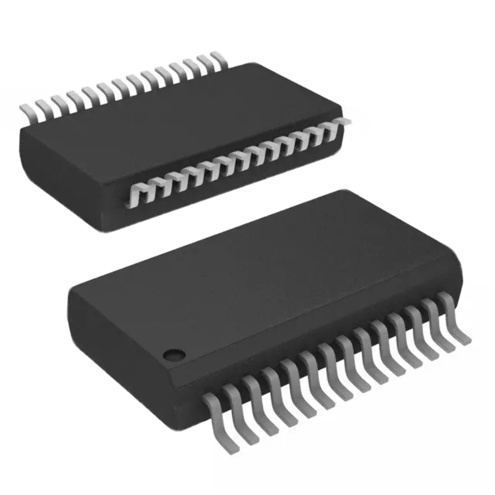
ADM560JRS is a low power RS 232 transceiver designed for systems that exchange serial data between logic circuits and standard RS 232 communication lines. The device integrates four transmitters and five receivers, allowing multiple signal paths within a single compact package. It operates from a single 3 V to 3.6 V supply and generates the required positive and negative interface voltages using an internal charge pump with external capacitors. Data transfer rates reach 116 kbps, supporting typical serial communication tasks. The device is packaged in a 28 pin SSOP format suited for surface mounted circuit boards. Looking for ADM560JRS? Contact us to check current stock, lead time, and pricing.
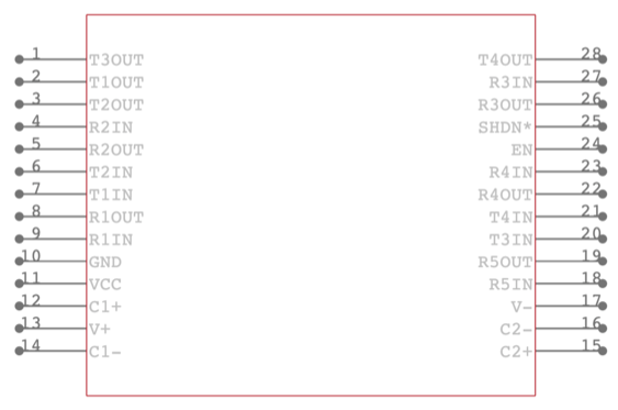
ADM560JRS Pinout Details
![[IMAGE OF PINOUT]](/upfile/images/af/20260305192709105.png)
ADM560JRS Pin Description
| Pin Number | Pin Name | Description |
| 1 | T3OUT | RS-232 transmitter output channel 3 that drives the external serial line using RS-232 voltage levels. |
| 2 | T1OUT | RS-232 transmitter output channel 1 providing converted logic signals for serial communication lines. |
| 3 | T2OUT | RS-232 transmitter output channel 2 that outputs RS-232 compliant voltage signals. |
| 4 | R2IN | RS-232 receiver input channel 2 that accepts incoming RS-232 signals from external devices. |
| 5 | R2OUT | CMOS/TTL logic output corresponding to receiver channel 2 after RS-232 level conversion. |
| 6 | T2IN | Logic level input for transmitter channel 2 that is converted internally to RS-232 output levels. |
| 7 | T1IN | Logic level input for transmitter channel 1 used to drive the RS-232 output stage. |
| 8 | R1OUT | Logic level output from receiver channel 1 representing the converted RS-232 input signal. |
| 9 | R1IN | RS-232 receiver input channel 1 connected to an external serial interface line. |
| 10 | GND | Ground reference for the device and internal circuitry. |
| 11 | VCC | Main power supply input, typically operating from approximately 3.0 V to 3.6 V. |
| 12 | C1+ | Positive terminal of the first charge pump capacitor used in the voltage doubler stage. |
| 13 | V+ | Positive generated voltage output from the internal charge pump used by RS-232 drivers. |
| 14 | C1− | Negative terminal of the first charge pump capacitor used in the voltage doubler circuit. |
| 15 | C2+ | Positive terminal of the second charge pump capacitor used for the voltage inverter stage. |
| 16 | C2− | Negative terminal of the second charge pump capacitor used to generate the negative RS-232 voltage. |
| 17 | V− | Negative voltage output from the internal charge pump used for RS-232 signaling. |
| 18 | R5IN | RS-232 receiver input channel 5 for incoming serial data signals. |
| 19 | R5OUT | CMOS/TTL logic output corresponding to receiver channel 5 after signal conversion. |
| 20 | T3IN | Logic level input for transmitter channel 3 used to produce RS-232 output signals. |
| 21 | T4IN | Logic level input for transmitter channel 4 that feeds the internal RS-232 driver stage. |
| 22 | R4OUT | Logic level output from receiver channel 4 representing the converted RS-232 input signal. |
| 23 | R4IN | RS-232 receiver input channel 4 connected to an external communication line. |
| 24 | EN | Enable control input used to activate or deactivate the device’s internal circuitry. |
| 25 | SHDN | Shutdown control input that places the device into a low power shutdown mode. |
| 26 | R3OUT | Logic level output from receiver channel 3 corresponding to the received RS-232 signal. |
| 27 | R3IN | RS-232 receiver input channel 3 for receiving serial interface signals. |
| 28 | T4OUT | RS-232 transmitter output channel 4 providing converted serial output signals. |
ADM560JRS CAD Model
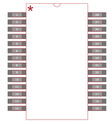
ADM560JRS Symbol
ADM560JRS Footprint
ADM560JRS 3D Model
Features of ADM560JRS
Integrated RS232 Transceiver Structure
The ADM560JRS combines four transmitters and five receivers within one compact device. This arrangement supports full duplex serial communication while reducing the number of separate interface components required on a circuit board.
Single Low Voltage Supply Operation
The device operates from a single supply between 3 V and 3.6 V. This allows it to connect directly to modern low voltage logic systems without requiring additional power rails.
Internal Charge Pump Voltage Generation
An internal charge pump creates the positive and negative voltages needed for RS 232 signaling. External capacitors connected to dedicated pins assist the circuit in generating stable interface voltage levels.
Multiple Receiver Channels
Five independent receiver channels accept RS 232 input signals and convert them into logic level outputs. This allows several communication lines to be monitored and processed within one integrated circuit.
Four Dedicated Transmitter Outputs
Four transmitter paths convert logic level input signals into RS 232 output levels. These outputs drive external communication lines that connect to serial ports or other interface devices.
Receiver Noise Tolerance
Each receiver channel includes hysteresis at the input stage. This design helps maintain stable logic output when the incoming signal contains electrical noise or slow transitions.
Data Transfer Support up to 116 kbps
The device supports data rates up to 116 kilobits per second. This range covers common serial communication speeds used in control equipment and computer interfaces.
Compact Surface Mount Package
The device is provided in a 28 lead SSOP package. Its small footprint supports dense circuit layouts while maintaining clear pin spacing for reliable assembly.
ADM560JRS Technical Specifications
| Product Attribute | Attribute Value |
| Manufacturer | Analog Devices, Inc. |
| Voltage - Supply | 3V ~ 3.6V |
| Type | Transceiver |
| Supplier Device Package | 28-SSOP |
| Series | - |
| Receiver Hysteresis | 300 mV |
| Protocol | RS232 |
| Package / Case | 28-SSOP (0.209', 5.30mm Width) |
| Package | Tube |
| Operating Temperature | 0°C ~ 70°C |
| Number of Drivers/Receivers | 4/5 |
| Mounting Type | Surface Mount |
| Duplex | Full |
| Data Rate | 116Kbps |
| Base Product Number | ADM560 |
| Moisture Sensitivity Level (MSL) | 1 (Unlimited) |
| ECCN | EAR99 |
| HTSUS | 8542.39.0001 |
Functional Block Diagram of ADM560JRS
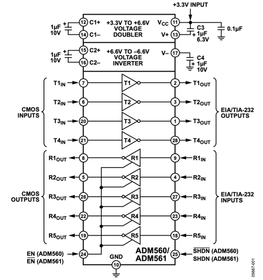
Internal structure organizes the ADM560JRS into power generation, transmitter, and receiver sections that convert logic signals to RS-232 levels and back. A charge pump stage at the top produces positive and negative supply rails from a single +3.3 V input using external capacitors connected to C1 and C2 pins, generating V+ and V− voltages used by the interface drivers. Four transmitter paths accept CMOS inputs labeled T1IN through T4IN and drive RS-232 outputs T1OUT through T4OUT. Five receiver paths accept RS-232 inputs labeled R1IN through R5IN and translate them into CMOS outputs R1OUT through R5OUT. Control and reference pins including EN or SHDN, VCC, and GND appear at the lower portion of the layout, indicating device enable control and power connections while grouping the signal flow between CMOS logic and EIA/TIA-232 communication lines.
Applications of ADM560JRS
Personal Computer Serial Interfaces
The ADM560JRS can connect logic circuits in computers or embedded controllers to RS 232 serial ports. Its transmitters and receivers manage signal level conversion so digital logic can communicate with external devices that use standard serial communication lines.
Industrial Control Equipment
Control units in industrial environments often exchange data with sensors, controllers, or diagnostic tools through serial links. The device allows these systems to interface with RS 232 communication ports while keeping the internal logic operating at low voltage levels.
Communication Terminals and Modems
Many communication terminals and modem based systems rely on RS 232 signaling between processing circuits and external communication equipment. The device handles signal translation between logic circuits and the serial interface used by these systems.
Medical Monitoring and Diagnostic Devices
Medical instruments sometimes exchange configuration data or measurement results through serial connections. The ADM560JRS provides stable signal conversion that allows microcontroller based medical equipment to communicate with external computers or data recorders.
Portable Data Logging Equipment
Portable monitoring systems and handheld instruments may use serial links to transfer stored measurements to other devices. The device allows these battery powered systems to maintain reliable RS 232 communication while operating from low voltage supplies.
Embedded Systems with Legacy Serial Links
Embedded control systems used in automation or testing often interact with older equipment that communicates through RS 232. The ADM560JRS enables modern digital circuits to maintain compatibility with these established serial communication interfaces.
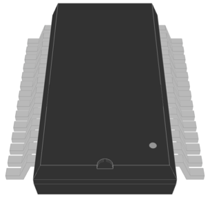
Outline Dimensions of ADM560JRS
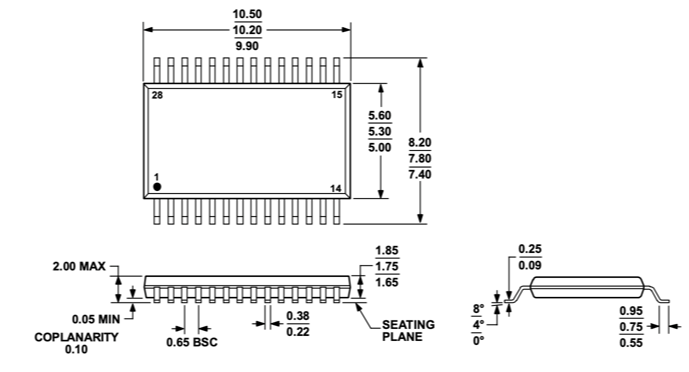
Physical package layout presents the 28 lead shrink small outline package used for the ADM560JRS with dimensions expressed in millimeters. The top view indicates the rectangular body with leads arranged along both long sides and pin numbering beginning at the corner marked with a dot. Body length ranges from 9.90 mm to 10.50 mm and body width ranges from 5.00 mm to 5.60 mm, while the overall span including leads extends approximately 7.40 mm to 8.20 mm. Lead pitch is specified as 0.65 mm between adjacent pins, supporting compact surface mounting. Side and end profiles show the seating plane, lead bend angle, and coplanarity tolerance, with maximum package height near 2.00 mm. Additional measurements define lead width, lead thickness, and terminal extension to ensure compatibility with standard SSOP land patterns defined by JEDEC MO-150-AH.
Advantages and Disadvantages of ADM560JRS
Advantages
• Provides multiple drivers and receivers in a single integrated device, reducing component count
• Low supply voltage operation suitable for modern low-power systems
• Integrated charge pump eliminates the need for external ±RS-232 supply voltages
• Receiver hysteresis improves reliability in electrically noisy environments
• Compact surface-mount package helps minimize board space usage
• Supports standard RS-232 communication making it widely compatible with serial devices
• Low power consumption suitable for battery-powered equipment
Disadvantages
• Maximum data rate limited to 116 kbps, which is slower compared to modern high-speed interfaces
• Operating temperature range is limited to commercial grade (0°C to 70°C)
• Requires external capacitors for charge pump operation
• Designed specifically for RS-232, which is considered a legacy communication standard
• Product is obsolete and no longer in active production
ADM560JRS Alternatives
| Part Number | Manufacturer | Key Features | Use Case/Notes |
| ADM560JRSZ | Analog Devices Inc. | Packaged in a 196-LFBGA form factor designed for compact, high-density electronic assemblies. It supports surface-mount installation and reliable operation across a wide industrial temperature range from −40°C to 85°C, helping maintain stable performance in demanding circuits. | Used in advanced electronic systems that require compact packaging and dependable performance. Suitable for industrial and embedded designs where stable operation and efficient board space usage are important. |
| ADM560JRS-REEL | Analog Devices Inc. | Supplied in a 16-PDIP package designed for through-hole mounting. The package style allows straightforward installation and easy handling during assembly or testing. It operates within a typical commercial temperature range of 0°C to 70°C. | Commonly used in development boards, prototypes, or equipment that uses through-hole components. The DIP format also makes troubleshooting, replacement, and manual assembly simpler. |
| ADM560JR | Analog Devices Inc. | Encased in a compact 64-VQFN package with an exposed thermal pad. Designed for surface-mount assembly, it supports reliable operation from −40°C to 85°C while improving heat dissipation and electrical grounding. | Well suited for modern embedded systems and industrial electronics where compact size and efficient thermal management are required. Often used in high-density circuit designs. |
About Analog Devices, Inc.
Analog Devices, Inc. is a semiconductor company that develops integrated circuits used for signal processing, data conversion, and interface communication. Founded in 1965 and headquartered in the United States, the company focuses on analog, mixed signal, and digital signal processing technologies. Its products are widely used in industrial systems, communication equipment, healthcare instruments, automotive electronics, and consumer devices. The company’s portfolio includes amplifiers, data converters, interface circuits, power management devices, and signal processing components designed for electronic systems that require precise and reliable signal handling.
Conclusion
The ADM560JRS is designed to handle serial communication between logic circuits and RS232 devices. You get four transmitters and five receivers in one package, which allows several signal lines to be managed at the same time. Its internal charge pump creates the required interface voltages from a single low voltage supply. The compact SSOP package helps keep circuit layouts small and organized. You can apply the device in control systems, computer interfaces, and communication equipment that rely on RS232 data exchange. With its integrated structure, it reduces the need for extra interface components.
Datasheet PDF
ADM560JRS Datasheet:
About us
ALLELCO LIMITED
Read more
Quick inquiry
Please send an inquiry, we will respond immediately.
Frequently Asked Questions [FAQ]
1. What does the ADM560JRS do?
ADM560JRS converts logic level signals to RS232 voltage levels and converts incoming RS232 signals back to logic levels, allowing digital systems to communicate through serial ports.
2. How many transmitters and receivers are included in ADM560JRS?
The device contains four transmitters and five receivers, allowing multiple RS232 communication lines to be handled within a single integrated circuit.
3. What power supply does ADM560JRS use?
ADM560JRS operates from a single power supply between 3 V and 3.6 V while generating the required RS232 voltages internally through a charge pump.
4. What type of package does ADM560JRS use?
The device is packaged in a 28 pin SSOP surface mount package designed for compact circuit board layouts.
5. Where is ADM560JRS commonly used?
It is used in systems that communicate through RS232 serial connections, such as computer interfaces, industrial control units, communication equipment, and embedded devices.
Understanding the XC2S200-5FG256I FPGA Architecture and Applications
on March 5th
How the XCV300E-7FG456I FPGA Supports Digital System Design
on March 5th
Popular Posts
-

Complex Instruction Set Computers: How They Changed Computing?
on April 18th 147754
-

USB-C Pinout and Features
on April 18th 111931
-

Using Xilinx Unified Simulation Primitives: A Comprehensive Guide to FPGA Design and Simulation
on April 18th 111349
-

Power Supply Voltages in Electronics: Meaning of VCC, VDD, VEE, VSS, and GND
on April 18th 83718
-

RJ45 Connector Guide: Pinout, Wiring, Cable Types, and Uses
on January 1th 79505
-

The Ultimate Guide to Wire Color Codes in Modern Electrical Systems
The way our electrical systems use colors isn’t just for looks. Each wire color now indicates a specific function, making it easier to identify and handle electrical components correctly during ins...on January 1th 66873
-

Quality (Q) Factor: Equations and Applications
The quality factor, or 'Q', is important when checking how well inductors and resonators work in electronic systems that use radio frequencies (RF). 'Q' measures how well a circuit minimizes energy...on January 1th 63010
-

Purge Valve Guide: Function, Symptoms, Testing, and Replacement for Optimal Engine Performance
The purge valve is a key part of a car’s system that helps keep the air clean by managing fuel vapors before they can escape into the atmosphere. This not only helps the environment by reducing pol...on January 1th 62960
-

Achieving Peak Performance with the Maximum Power Transfer Theorem
The Maximum Power Transfer Theorem explains how energy from a source, such as a battery or generator, flows to a connected load. It shows the exact condition where the load receives the most power....on January 1th 54080
-

A23 Battery Specifications and Compatibility
The A23 battery is a small, cylinder-shaped battery with high voltage. Also called 23A, 23AE, or MN21, it runs at 12 volts and much higher than AA or AAA batteries. Its special design make...on January 1th 52101
HOT Part Number
-
7443551181
Würth Elektronik
FIXED IND 18UH 7.5A 22 MOHM SMD
LM4040C50IDCKR
Texas Instruments
IC VREF SHUNT 0.5% SC70-5
TPS76338DBVR
Texas Instruments
IC REG LINEAR 3.8V 150MA SOT23-5
MC908GZ32MFAE
NXP USA Inc.
IC MCU 8BIT 32KB FLASH 48LQFP
MUR1620CT
onsemi
DIODE ARRAY GP 200V 8A TO220AB
CA3140T
Rochester Electronics, LLC
IC OPAMP GP 1 CIRCUIT TO99-8
ISL6217ACV-T
Renesas Electronics America Inc
IC REG CTRLR INTEL 1OUT 38TSSOP
MMDF2P02ER2G
onsemi
MOSFET 2P-CH 25V 2.5A 8SOIC
MAX17543ATP+
Analog Devices Inc./Maxim Integrated
IC REG BUCK ADJ 2.5A 20TQFN
FTR-110-03-G-D-LC-06
Samtec Inc.
CONN HEADER SMD 20POS 1.27MM
HMC826LP6CETR
Analog Devices Inc.
IC PLL W/VCO FRACTIONAL-N 40SMD
NJM386M
Nisshinbo Micro Devices Inc.
IC AUDIO PWR AMP BIPO LV 8DMP
P6SMB12AT3
onsemi
TVS DIODE 10.2VWM 16.7VC SMB
BD82001FVJ-E2
Rohm Semiconductor
IC PWR SWITCH N-CHAN 1:1 8TSSOP
TLE2142ACD
Texas Instruments
IC OPAMP GP 2 CIRCUIT 8SOIC
2225SC101KAT1A\SB
KYOCERA AVX
CAP CER 100PF 1.5KV X7R 2225
AON6414AL
Alpha & Omega Semiconductor Inc.
MOSFET N-CH 30V 13A/30A 8DFN
0452001.MRL
Littelfuse Inc.
FUSE BRD MNT 1A 125VAC/VDC 2SMD -

P6SMB550A
Bourns Inc.
TVS DIODE 495VWM 760VC DO214AA
PIC18F23K20T-I/SS
Microchip Technology
IC MCU 8BIT 8KB FLASH 28SSOP
GRM1555C1H5R1BA01D
Murata Electronics
CAP CER 5.1PF 50V C0G/NP0 0402
MC9S08AC60MPUE
NXP USA Inc.
IC MCU 8BIT 60KB FLASH 64LQFP
KA317TU
onsemi
IC REG LIN POS ADJ 1.5A TO220-3
DMP2120U-13
Diodes Incorporated
MOSFET P-CH 20V 3.8A SOT23 T&R 1
CD74HC30M96
Texas Instruments
IC GATE NAND 1CH 8-INP 14SOIC
PIC16F570T-I/SS
Microchip Technology
IC MCU 8BIT 3KB FLASH 28SSOP
NE5230DG
onsemi
IC OPAMP GP 1 CIRCUIT 8SOIC
BCM33843ZUKFSBGB0T
Broadcom Limited
CABLE MODEM
06035C682KAT7A
KYOCERA AVX
CAP CER 6800PF 50V X7R 0603
BCR135SH6327XTSA1
Infineon Technologies
TRANS 2NPN PREBIAS 0.25W SOT363
CD74AC151M96
Texas Instruments
IC MULTIPLEXER 1 X 8:1 16SOIC
MAX44267AUD+
Analog Devices Inc./Maxim Integrated
IC OPAMP GP 2 CIRCUIT 14TSSOP
MB85RC16PNF-G-JNERE1
Kaga FEI America, Inc.
IC FRAM 16KBIT I2C 1MHZ 8SOP
HLMP-1401
Broadcom Limited
LED YELLOW DIFFUSED T-1 T/H
UCC2580D-4
Unitrode
IC OFFLINE SW MULT TOP 16SOIC
87832-0826
Molex
MGRID HDR SHRD SMT /LCK/CAP .38A -
UCC25705DGKTRG4
Texas Instruments
IC REG CTRLR MULT TOP 8VSSOP
FMMT3906TA
Diodes Incorporated
TRANS PNP 40V 0.2A SOT23-3
STU40N2LH5
STMicroelectronics
MOSFET N-CH 25V 40A IPAK
FSAM10SH60
onsemi
IC SMART POWER MOD 10A SPM32-AA
RT0603FRE071KL
Yageo
RES SMD 1K OHM 1% 1/10W 0603
ZX62-B-5PA(33)
Hirose Electric Co Ltd
CONN RCPT USB2.0 MICRO B SMD R/A
GBPC3506-E4/51
Vishay General Semiconductor - Diodes Division
BRIDGE RECT 1PHASE 600V 35A GBPC
SQA401EEJ-T1_GE3
Vishay Siliconix
MOSFET P-CH 20V 2.68A PPAK SC70
XC6221A182MR-G
Torex Semiconductor Ltd
IC REG LINEAR 1.8V 200MA SOT25
IRFH4210TRPBF
Infineon Technologies
MOSFET N-CH 25V 45A PQFN
L78L05ACD
STMicroelectronics
IC REG LINEAR 5V 100MA 8SO
04023J2R7BBSTR
KYOCERA AVX
CAP THIN FILM 2.7PF 25V 0402
C0603C0G1E750J
TDK Corporation
CAP CER 75PF 25V C0G 0201
SA20CA-E3/73
Vishay General Semiconductor - Diodes Division
TVS DIODE 20VWM 32.4VC DO204AC
PLL1705S1DBQR
Texas Instruments
PROTOTYPE
2SA2071T100Q
Rohm Semiconductor
TRANS PNP 60V 3A MPT3
XF3H-3555-31AR
Omron Electronics Inc-EMC Div
CONN FPC BOTTOM 35POS 0.3MM R/A
CY7C0851AV-133BBI
Infineon Technologies
IC SRAM 2MBIT 133MHZ 172FBGA