Understanding the XC2S200-5FG256I FPGA Architecture and Applications
You may be looking for a programmable logic device that lets you shape digital hardware exactly the way your system needs it. The XC2S200-5FG256I FPGA gives you flexible logic blocks, internal memory, and many input and output connections so you can build custom digital functions inside one device. Its architecture supports signal routing, timing control, and interface handling across many types of electronic equipment. With programmable routing and memory resources available on the chip, you can adapt it to different control tasks, communication paths, and embedded system functions without changing the physical hardware.Catalog
XC2S200-5FG256I Overview
The XC2S200-5FG256I is a programmable logic device built on the Spartan II FPGA architecture and designed for configurable digital systems. It provides around 200000 logic gates arranged through configurable logic blocks that can be programmed to implement custom digital functions. Integrated block RAM supports temporary data storage, while a large number of input and output pins allow flexible communication with external components. The device operates from a low voltage core supply and supports industrial temperature conditions. Its architecture supports hardware prototyping, interface control, and digital processing tasks in embedded electronic equipment.
Looking for XC2S200-5FG256I? Contact us to check current stock, lead time, and pricing.
XC2S200-5FG256I b
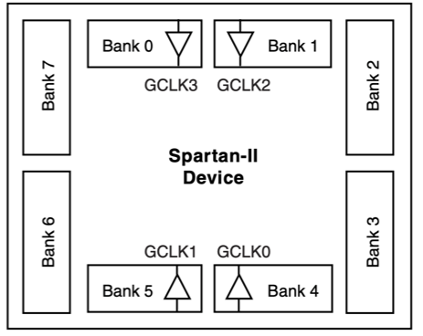
I/O structure divides the device perimeter into eight banks positioned along all four sides of the FPGA package. Each bank groups a set of input and output pins that share the same VCCO supply, allowing a consistent voltage level to be applied to all pins within that region. Global clock inputs labeled GCLK0 through GCLK3 are placed near the lower and upper sections of the layout to distribute clock signals evenly across the internal logic array. This arrangement enables multiple signaling standards to operate simultaneously by assigning different voltage levels to separate banks while maintaining organized routing between external pins and the internal programmable logic.
XC2S200-5FG256I CAD Model
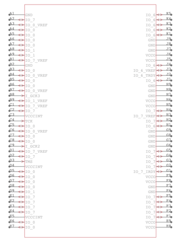
XC2S200-5FG256I Symbol
XC2S200-5FG256I Footprint

XC2S200-5FG256I 3D Model
Features of XC2S200-5FG256I
Programmable FPGA Logic Architecture
The device uses a configurable logic structure that allows digital circuits to be defined through programmable logic blocks and routing paths. This structure allows designers to implement custom hardware behavior without modifying the physical device, supporting flexible digital system development and hardware prototyping.
Integrated Block Memory Resources
Internal block RAM provides dedicated memory storage within the programmable fabric. These memory blocks support data buffering, lookup tables, and temporary storage operations, reducing the need for external memory components in many digital processing applications.
Configurable Input and Output Interface
Up to 176 user input and output pins provide flexible connectivity with external devices. Each pin can be configured for different input, output, or bidirectional functions, allowing the device to interact with sensors, communication interfaces, and control systems.
Programmable Routing Network
A programmable interconnection network links logic blocks, memory elements, and input output interfaces. Signals can be routed through configurable paths, allowing custom signal flow between internal resources while maintaining predictable digital behavior.
Clock Management Using Delay Locked Loops
Integrated delay locked loop circuits support clock distribution and timing alignment inside the device. These circuits help maintain stable timing relationships between internal logic sections and external clock sources.
Industrial Temperature Operating Capability
The device supports operation across an extended temperature range suitable for industrial environments. This allows stable performance in systems exposed to varying environmental conditions such as factory equipment or outdoor installations.
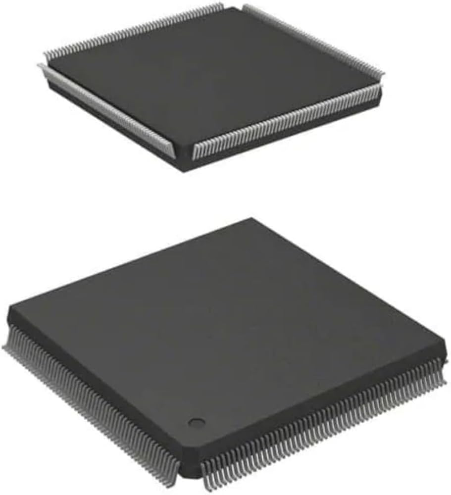
Compact Surface Mount BGA Package
The device is packaged in a 256 ball grid array format that allows a high number of connections in a compact footprint. This packaging style supports dense printed circuit board layouts while maintaining electrical reliability for high pin count devices.
XC2S200-5FG256I Technical Specifications
| Product Attribute | Attribute Value |
| Manufacturer | AMD Xilinx |
| Voltage - Supply | 2.375V ~ 2.625V |
| Total RAM Bits | 57344 |
| Supplier Device Package | 256-FBGA (17x17) |
| Series | Spartan®-II |
| Package / Case | 256-BGA |
| Package | Tray |
| Operating Temperature | -40°C ~ 100°C (TJ) |
| Number of Logic Elements/Cells | 5292 |
| Number of LABs/CLBs | 1176 |
| Number of I/O | 176 |
| Number of Gates | 200000 |
| Mounting Type | Surface Mount |
| Base Product Number | XC2S200 |
| RoHs Status | RoHS non-compliant |
| Moisture Sensitivity Level (MSL) | 3 (168 Hours) |
| REACH Status | REACH Unaffected |
| ECCN | EAR99 |
| HTSUS | 8542.39.0001 |
Block Diagram of XC2S200-5FG256I
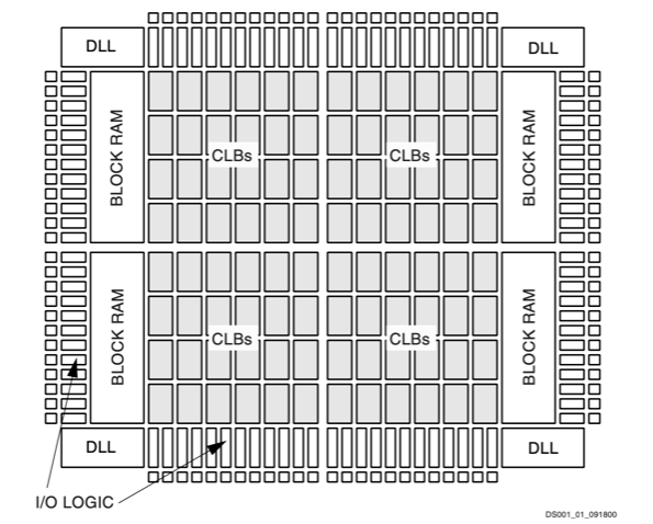
Central grid of Configurable Logic Blocks forms the programmable logic fabric where digital functions are implemented using lookup tables and flip flops. Vertical columns labeled block RAM provide embedded memory resources placed alongside the logic array for data storage and buffering operations. Input and output logic blocks line the outer edges of the device and connect the internal routing network to external pins. Delay locked loop units located at the corners support clock alignment and timing control across the internal logic structure. Interconnection paths between the CLB array, memory columns, clock units, and I O blocks create the programmable routing network that enables flexible signal connections throughout the device.
Input/Output Block (IOB) of XC2S200-5FG256I
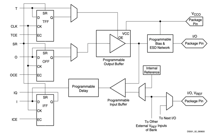
Internal I/O block structure connects external package pins to the programmable logic fabric through configurable input and output paths. Output data passes through a flip flop labeled OFF with clock and enable control, followed by a programmable output buffer that drives the external pin while operating from the VCCO supply associated with the I O bank. Input signals from the package pin enter through a programmable input buffer and optional programmable delay stage before reaching an input flip flop labeled IFF that synchronizes the signal with the internal clock. Additional control elements include tri state control through the TFF register, clock enable signals, and set reset inputs that manage signal timing and state control. A programmable bias and ESD protection network safeguards the pin interface, while an internal reference and VREF connections support voltage referenced I O standards shared across the bank.
Applications of XC2S200-5FG256I
Digital Signal Routing Systems
Programmable logic resources allow the device to manage digital signal routing and processing in communication equipment. Its configurable logic blocks can implement custom logic paths that handle data transfer between system components while maintaining stable timing behavior.
Industrial Automation Control Units
Industrial control systems often require flexible digital logic that can adapt to different machine processes. The device can manage control signals, sensor inputs, and actuator outputs, supporting reliable operation in automated production environments.
Embedded Hardware Prototyping Platforms
Development platforms frequently use programmable logic devices to test digital designs before final hardware production. The device allows designers to implement and modify logic structures during development, enabling efficient testing of digital control functions.
Communication Interface Bridging
Systems that connect multiple communication protocols can use the device to translate or route digital signals between interfaces. Its programmable logic allows custom data paths that link processors, memory devices, and communication controllers.
Automotive Electronic Subsystems
Electronic control units in vehicles require programmable logic for signal management and system coordination. The device can handle digital control tasks, communication interfaces, and timing functions within automotive electronics.
Consumer Electronic Control Logic
Digital consumer devices often require compact programmable logic to manage system functions. The device can coordinate user interface signals, timing control, and internal communication between components within electronic products.
XC2S200-5FG256I Advantages and Disadvantages
Advantages
• Programmable logic structure allows digital circuits to be reconfigured after installation
• Integrated block memory supports data storage without external memory in some designs
• Large number of input and output pins supports flexible system connectivity
• Stable operation across industrial temperature conditions
• Compact BGA package supports dense printed circuit board layouts
• Internal clock alignment circuits help maintain consistent timing behavior
Disadvantages
• Logic capacity is lower than that of more recent programmable devices
• On chip memory size is limited compared with modern programmable logic families
• Power consumption can be higher than newer low voltage architectures
• Does not include advanced integrated signal processing resources
• Requires external configuration memory for device programming
XC2S200-5FG256I Alternatives
| Part Number | Manufacturer | Key Features | Use Case/Notes |
| XC2S200-5FGG256I | AMD | Spartan-II FPGA with configurable logic blocks, distributed RAM, and programmable routing resources. It operates around a 2.5 V core supply and provides thousands of logic cells for implementing custom digital circuits. | Used in embedded processing, industrial control, and communication hardware where programmable logic and reliable operation in industrial temperature ranges are required. |
| XC2S200-5FGG256C | AMD | FPGA device from the Spartan-II family that integrates programmable logic elements, internal memory blocks, and configurable I/O connections for flexible digital design. | Suitable for consumer electronics, communication modules, and prototyping platforms where moderate logic density and flexible hardware configuration are required. |
| XC2S200-5FG256C | AMD | Programmable FPGA device offering configurable logic cells, internal memory resources, and multiple user-configurable I/O pins to implement complex digital circuits on a single chip. | Applied in data acquisition systems, signal processing platforms, and embedded designs that need programmable digital hardware. |
| XC2S200-5FGG456I | AMD | High-pin-count Spartan-II FPGA providing programmable logic blocks, embedded memory, and a large number of I/O connections for complex digital systems. | Used in industrial automation, advanced communication equipment, and high-I/O embedded systems requiring flexible programmable logic and extended temperature support. |
About AMD Xilinx
AMD Xilinx is a semiconductor technology company known for the development of programmable logic devices and adaptive computing platforms. The company originated as Xilinx and later became part of Advanced Micro Devices. Its work focuses on field programmable gate arrays, adaptive system on chip devices, and programmable acceleration platforms used in computing, communications, automotive electronics, and industrial systems. The company has developed programmable logic architectures for several decades, supporting digital hardware design through configurable devices that allow circuits to be defined after manufacturing. Its products are widely used in embedded systems, network infrastructure, signal processing equipment, and electronic control systems.
Conclusion
The XC2S200-5FG256I FPGA gives you a flexible way to build digital logic directly in hardware. You can configure its logic blocks, memory resources, and input and output connections to support different system tasks. Its internal structure allows signal routing, timing control, and data storage inside a single programmable device. With its configurable aUnderstanding the XC2S200-5FG256I FPGA Architecture and Applicationsrchitecture, the device can support embedded electronics, communication interfaces, and control systems. Understanding its layout, features, and applications helps you see how programmable logic devices support modern digital equipment. This makes it easier for you to evaluate whether the XC2S200-5FG256I fits the needs of your electronic design.
Datasheet PDF
XC2S200-5FG256I Datasheet:
About us
ALLELCO LIMITED
Read more
Quick inquiry
Please send an inquiry, we will respond immediately.
Frequently Asked Questions [FAQ]
1. What type of device is XC2S200-5FG256I
XC2S200-5FG256I is a field programmable gate array. It is a programmable logic device that allows digital circuits to be configured through software rather than fixed hardware design.
2. How many input and output pins does XC2S200-5FG256I provide
The XC2S200-5FG256I device supports up to 176 user configurable input and output pins, allowing it to connect with many external components and communication interfaces.
3. What is the purpose of block RAM in the XC2S200 FPGA
Block RAM provides internal memory used for temporary data storage, buffering, lookup tables, and other data handling tasks within the programmable logic system.
4. Where is the XC2S200-5FG256I commonly used
This device is often used in embedded electronics, communication systems, industrial automation equipment, and digital control systems that require programmable hardware logic.
5. What package type does the XC2S200-5FG256I use
The XC2S200-5FG256I is packaged in a 256 ball grid array format, which allows a large number of connections in a compact footprint suitable for dense circuit board layouts.
Understanding DVI Connectors: Everything You Need to Know
on March 9th
ADM560JRS Interface Chip Guide, Features, and Applications
on March 5th
Popular Posts
-

Complex Instruction Set Computers: How They Changed Computing?
on April 17th 147710
-

USB-C Pinout and Features
on April 17th 111653
-

Using Xilinx Unified Simulation Primitives: A Comprehensive Guide to FPGA Design and Simulation
on April 17th 111314
-

Power Supply Voltages in Electronics: Meaning of VCC, VDD, VEE, VSS, and GND
on April 17th 83575
-

RJ45 Connector Guide: Pinout, Wiring, Cable Types, and Uses
on January 1th 79216
-

The Ultimate Guide to Wire Color Codes in Modern Electrical Systems
The way our electrical systems use colors isn’t just for looks. Each wire color now indicates a specific function, making it easier to identify and handle electrical components correctly during ins...on January 1th 66745
-

Quality (Q) Factor: Equations and Applications
The quality factor, or 'Q', is important when checking how well inductors and resonators work in electronic systems that use radio frequencies (RF). 'Q' measures how well a circuit minimizes energy...on January 1th 62923
-

Purge Valve Guide: Function, Symptoms, Testing, and Replacement for Optimal Engine Performance
The purge valve is a key part of a car’s system that helps keep the air clean by managing fuel vapors before they can escape into the atmosphere. This not only helps the environment by reducing pol...on January 1th 62792
-

Achieving Peak Performance with the Maximum Power Transfer Theorem
The Maximum Power Transfer Theorem explains how energy from a source, such as a battery or generator, flows to a connected load. It shows the exact condition where the load receives the most power....on January 1th 54020
-

A23 Battery Specifications and Compatibility
The A23 battery is a small, cylinder-shaped battery with high voltage. Also called 23A, 23AE, or MN21, it runs at 12 volts and much higher than AA or AAA batteries. Its special design make...on January 1th 51936
HOT Part Number
-

R5010810XXWA
Powerex Inc.
DIODE GP REV 800V 100A DO205AA
0603YG274ZAT2A
KYOCERA AVX
CAP CER 0.27UF 16V Y5V 0603
MCIMX283CVM4B
NXP USA Inc.
IC MPU I.MX28 454MHZ 289MAPBGA
MC74ACT373DW
onsemi
IC LATCH OCT TRANSP 3ST 20-SOIC
FODM121CR2V
Fairchild Semiconductor
TRANSISTOR OUTPUT OPTOCOUPLER, 3
ISO7420FEDR
Texas Instruments
DGTL ISO 2500VRMS 2CH GP 8SOIC
MAX507ACWG
Analog Devices Inc./Maxim Integrated
IC DAC 12BIT V-OUT 24SOIC
MAX765CSA
Analog Devices Inc./Maxim Integrated
IC REG BCK BST ADJ/-12V 8SOIC
SN65240PWRG4
Texas Instruments
IC USB TRANSIENT SUPP 8-TSSOP
LCA125LSTR
IXYS Integrated Circuits Division
SSR RELAY SPST-NO 170MA 0-350V
R5F1057AANA#20
Renesas Electronics America Inc
IC MCU 16BIT 16KB FLASH 24HWQFN
LTC6244HMS8#PBF
Analog Devices Inc.
IC CMOS 2 CIRCUIT 8MSOP
JMK107BJ106MA-L
Taiyo Yuden
CAP CER 10UF 6.3V X5R 0603
GBU2510
Yangzhou Yangjie Electronic Technology Co.,Ltd
RECT BRIDGE 1000V 25A GBU
DSPIC33EP512GM710-I/BG
Microchip Technology
IC MCU 16BIT 512KB FLSH 121TFBGA
FAN1587AT
Fairchild Semiconductor
ADJUSTABLE LDO REGULATOR
NCP4641H033T1G
onsemi
IC REG LINEAR 3.3V 120MA SOT89-5
AP2181DFMG-7
Diodes Incorporated
IC PWR SWITCH P-CHANNEL 1:1 6DFN -

C3216X5R1H225M160AB
TDK Corporation
CAP CER 2.2UF 50V X5R 1206
GD25Q80CTIG
GigaDevice Semiconductor (HK) Limited
IC FLASH 8MBIT SPI/QUAD I/O 8SOP
ZL30361GDG2
Microchip Technology
IC NETWORK SYNCH ETH CLK 144LBGA
AP22814BM8-13
Diodes Incorporated
IC PWR SWITCH P-CHAN 1:1 8MSOP
FSBM20SH60A
Fairchild Semiconductor
AC MOTOR CONTROLLER, 40A, HYBRID
UPD44645364AF5-E40-FQ1-A
Renesas Electronics America Inc
STANDARD SRAM, 2MX36, 0.45NS
VESD16C1-02VHG3-08
Vishay General Semiconductor - Diodes Division
TVS DIODE 16VWM 28VC SOD523
UCC28084P
Texas Instruments
IC REG CTRLR MULT TOPOLOGY 8DIP
FQP30N06L
onsemi
MOSFET N-CH 60V 32A TO220-3
FTSH-107-01-L-DV-P-TR
Samtec Inc.
CONN HEADER SMD 14POS 1.27MM
MXA8-PW65-0000
Lumileds
LED LUXEON COOL WHITE 6500K 2SMD
TZ430N20KOF
International Rectifier (Infineon Technologies)
SCR MODULE 2KV 1050A MODULE
256-100
WAGO Corporation
END PLATE; SNAP-FIT TYPE; 1 MM T
ADS1115IRUGT
Texas Instruments
IC ADC 16BIT SIGMA-DELTA 10X2QFN
Z0107MN 5AA4
STMicroelectronics
TRIAC SENS GATE 600V 1A SOT223
DPG60C300HB
IXYS
DIODE ARRAY GP 300V 30A TO247AD
FDMC7660S
onsemi
MOSFET N-CH 30V 20A/40A POWER33
CKG32KX7T2E334K335AH
TDK Corporation
CAP CER 0.33UF 250V X7T SMD -

TPS61194PWPR
Texas Instruments
IC LED DRVR RGLTR PWM 20HTSSOP
MAX765EPA+
Analog Devices Inc./Maxim Integrated
IC REG BCK BST ADJ/-12V 8DIP
HMC174MS8TR
Analog Devices Inc.
IC RF SWITCH SPDT 3GHZ 8MSOP
BU4945G-TR
Rohm Semiconductor
IC SUPERVISOR 1 CHANNEL 5SSOP
D2425
Sensata-Crydom
SSR RELAY SPST-NO 25A 24-280V
GRM3166R1H220JZ01D
Murata Electronics
CAP CER 22PF 50V R2H 1206
STL23NS3LLH7
STMicroelectronics
MOSFET N-CH 30V 92A POWERFLAT
FAN5066MX
Fairchild Semiconductor
SWITCHING CONTROLLER
MAX3318IDBR
Texas Instruments
IC TRANSCEIVER FULL 2/2 20SSOP
IXTP10N60P
IXYS
MOSFET N-CH 600V 10A TO220AB
0603YG105ZAT2A
KYOCERA AVX
CAP CER 1UF 16V Y5V 0603
NSS40600CF8T1G
Rochester Electronics, LLC
NSS40600CF8 - TRANS BJTS PNP 40V
ZXMHC6A07N8TC
Diodes Incorporated
MOSFET 2N/2P-CH 60V 8-SOIC
1SMB85AT3G
Littelfuse Inc.
TVS DIODE 85VWM 137VC SMB
STP1612PW05MTR
STMicroelectronics
IC LED DRVR LINEAR PWM 60MA 24SO
LQP03TN3N2B02D
Murata Electronics
FIXED IND 3.2NH 450MA 250MOHM SM
GRM1555C1H9R6WZ01D
Murata Electronics
CAP CER 9.6PF 50V C0G/NP0 0402
CPH6003A-TL-E
onsemi
RF TRANS NPN 12V 7GHZ 6CPH