
Comprehensive Guide to ADC0804 ADC: Pinout, Schematic, and Usage
Analog-to-digital converters (ADCs) bridge the gap between the analog and digital worlds, making them requisite in modern electronics. By converting analog signals, such as voltage or current, into precise digital outputs, ADCs enable digital devices to process and interpret phenomena. As technology evolves, ADCs have become basic to microcontroller-based systems, influencing industries ranging from automation to consumer electronics. Among these, the ADC0804 stands out for its historical significance and versatility. This article explores the ADC0804's setup, circuit design, and applications, shedding light on its enduring relevance in analog-to-digital conversion.Catalog

ADC0804 Overview
The ADC0804 is an 8-bit CMOS converter that leverages the successive approximation method to achieve effective digital conversion. Designed for efficient communication with the 8080A control bus, its three-state outputs simplify processor interactions by functioning as memory locations or I/O ports, removing the requirement for extra interface hardware. Its integration with microcontrollers—take the Raspberry Pi for instance—is enhanced by built-in clock generation that alleviates the need for external timing signals. Offering an 8-bit resolution, this module becomes versatile across various applications, such as precise temperature monitoring, highlighting its substantial influence on modern technological ecosystems. Its extensive use emphasizes a profound sense of dependability and capability.
In our daily lives, outcomes frequently appear as continuous mathematical values, presenting challenges to systems crafted within discrete frequency domains. ADCs play a major part by converting analog inputs into discrete digital signals that electronic devices can swiftly process, thereby expanding their usability across different high-tech sectors. Everyday circumstances reinforce the necessity of this conversion, which allows complex systems to function without obstacles.

Pin Configuration
Contained within a 20-pin setup, every pin on the ADC0804 is designed for a distinct task, underpinning its efficient performance.

Pin Functions
|
Pin No. |
Pin Name |
Description |
|
1 |
Chip Select (CS) |
Chip select is used if more than one ADC module is used.
By default, grounded. |
|
2 |
Read (RD) |
Read pin must be grounded to read the Analog value. |
|
3 |
Write (WR) |
Write pin should be pulsed high to start data conversion. |
|
4 |
CLK IN |
External clock can be connected here, else RC can be used
for accessing internal clock. |
|
5 |
Interrupt (INTR) |
Goes high for interrupt request. |
|
6 |
Vin (+) |
Differential Analog input +. Connect to ADC input. |
|
7 |
Vin (-) |
Differential Analog input -. Connect to ground. |
|
8 |
Ground |
Analog Ground pin connected to ground of circuit. |
|
9 |
Vref/2 |
Reference voltage for ADC conversion. |
|
10 |
Ground |
Digital Ground pin connected to ground of circuit. |
|
11 to 18 |
Data bit 0 to bit 7 |
Seven output Data bit pins from which output is obtained. |
|
19 |
CLK R |
RC timing resistor input pin for internal clock
generation. |
|
20 |
Vcc |
Powers the ADC module, use +5V. |
Each pin in the ADC0804 assembly plays a part in the device's operations, allowing detailed interaction with external electronic components. The pin layout ensures smooth incorporation into numerous electronic systems, extending the ADC0804's utility across various scenarios.
Role of the Vref/2 Pin
The Vref/2 pin significantly shapes the ADC's reference voltage, influencing how input fluctuations are translated into digital form. When pin-9 is left unconnected, it permits operation within a 0 to 5 volts range, with conversion happening in steps of 19.6 mV. This characteristic aligns with tasks necessitating highly accurate measurements, as it influences both the ADC’s range and the resolution of its output. Recognizing these conversion steps aids in refining the design of systems that require meticulous digital representations of analog signals, highlighting their sensitivity and precision in practical applications.
Features of ADC0804
|
Feature |
Description |
|
Microprocessor Compatibility |
Seamless integration with all Microprocessors or
standalone operation. |
|
ADC Module |
Single-channel 8-bit ADC module. |
|
On-Chip Clock |
No external oscillator (clock) is required. |
|
Digital Output |
Ranges from 0 to 255. |
|
Input Voltage Range |
2.5V – 6.5V. |
|
Step Size |
With Vref set at 5V, each 19.53mV analog value increase
results in a one-bit rise. |
|
Package Options |
Available in 20-pin PDIP and SOIC packages. |
|
Conversion Time |
Analog to digital conversion takes 110 microseconds. |
|
Internal Clock Frequency |
Operates at 640 kilohertz. |
|
Voltage Measurement Capability |
Measures voltages from 0 to 5 volts with a 5V input
supply. |
|
Voltage Reference Compatibility |
Compatible with various voltage references, with a
minimum of 2.5V. |
|
Device Compatibility |
Fully functional with CMOS and TTL devices. |
|
Internal Clock |
Operating frequency at 640kHz. |
|
Zero Adjustment |
No need for zero adjustment during operation. |
|
Minimum Conversion Time |
110 microseconds. |
|
Differential Voltage Input |
Includes a differential analog voltage input. |
Circuit Diagram of the ADC0804
Functional Block Diagram

Internal Circuit
The ADC0804 performs the delicate task of converting analog signals into digital data, a procedure deeply ingrained in numerous scenarios demanding accurate measurement and regulation. To fully exploit this device, one must explore the fascinating interactions of electrons within. This exploration extends beyond mere signal conversion, encompassing the harmony of various sub-components working seamlessly together. Gaining a detailed understanding of this process can offer deep insights into maximizing performance, achieving both consistent efficiency and dependability in practical settings.
Encompassing a complex internal structure, the ADC0804 deploys an advanced network of gates, flip-flops, and decoders committed to signal transformation. The SAR (Successive Approximation Register) latch is key, executing a binary search algorithm to convert continuous analog inputs into accurate digital outputs. Required for this task is the coordinated operation of additional components, such as tri-state buffers and 8-bit shifters, which collectively ensure a structured and coherent data flow. Drawing on practical engineering experiences, fine-tuning these elements can considerably enhance conversion precision—mostly in environments where even minor discrepancies greatly affect outputs. Within the framework of complex systems, grasping these subtleties offers a tactical benefit in refining and adjusting to varied demands.
Integrating the ADC0804
Begin the integration sequence by engaging the ADC by pulling the CS pin to a low state. Next, initiate the analog-to-digital conversion by adjusting the WR pin. It is required to be attuned to the INTR pin; a low state reflects a completed conversion process. Access the digital output by adjusting the RD pin. Below is a C code example that sheds light on these procedural steps:
• Set `cs = 0;` // Engage the ADC by selecting the chip.
• `wr = 0;` // Indicate the start of a write operation.
• Introduce `delay(10);` // Allow ample time for signal stabilization.
• Set `wr = 1;` // Trigger the conversion process.
• Utilize a loop `while (intr == 1);` // Sustain waiting until conversion concludes.
• Set `rd = 0;` // Retrieve and read the conversion result.
The precision needed in timing and sequence is dominant for ensuring accurate data retrieval. Drawing from personal insights, meticulous attention to timing can deeply influence the reliability of the conversion results, akin to relying on rhythm to create harmonious tunes.
Proteus Circuit Demonstration

Within a detailed Proteus simulation, the adept conversion functionality of the ADC0804 is intensely demonstrated. The setup entails a connection between a variable voltage source and the ADC's analog input pins, unified by a common grounding. This setup ensures that digital outputs mirror changes in input signals with high fidelity.

For example, inputting around 4 volts typically results in a binary output of "11001100," which translates to a 3.9V analog output upon conversion. This nearly accurate analog reflection highlights the ADC0804's capability to translate analog signals into digital formats. Such simulations are used when fine-tuning systems for applications, emphasizing the invaluable role of experiential knowledge in achieving excellence in these conversions.
Applications for ADC0804
Platform Integration
The ADC0804 is famous for its adaptability, and it's frequently employed across various platforms, with remarkable use in the popular Raspberry Pi. Its seamless interfacing capability with a diverse array of input sources showcases its usefulness in projects centering on analog-to-digital conversion. Observations from numerous integration scenarios suggest that, when combined with platforms like Raspberry Pi, your interaction is simplified, inviting an enhanced experience through the delivery of precise digital outputs from analog signals. This symbiotic integration facilitates an environment where data processing is more streamlined, allowing for innovative developments in areas such as home automation and data collection.
Sensor and Transducer
The ADC0804, with its proficiency in sensor and transducer integration, is principally useful. It performs a dynamic function by converting analog signals from temperature sensors, pressure gauges, and various transducers into digital data manageable by contemporary microcontrollers. This harmony guarantees that the translated data maintains accuracy and responsiveness, which is invaluable in dynamic monitoring settings. Overcoming issues like signal noise becomes achievable through thoughtful circuit design and careful component selection, thereby assuring trustworthy data integrity.
Sensor Arrays
In the domain of sensor arrays, ADC0804 is highly valued for its capability to handle multiple inputs efficiently. Conventional circuit setups emphasize its productivity in projects necessitating synchronized data acquisition from numerous sensors. Implementing ADC0804 in such environments frequently results in scaling the capabilities of sensor networks. This application is mostly advantageous in environmental monitoring systems, where it is dynamic to continuously gather data from multiple locations.
Voltage Measurement and Indication
ADC0804 finds prominent use in voltage measurement and indicator systems, leveraging its aptitude for providing precise digital voltage level readouts in systems that require monitoring and control. Often utilized in educational labs and economical measurement setups, this application exemplifies the component's flexibility and accessibility for you at various levels. Strategic implementations reveal that coupling ADC0804 with additional components can enhance the visibility of voltage changes, facilitating proficient management of electrical systems.
ADC0804 Typical Application Schematic

Equivalent Models
• ADC0808
• MAX1112
Package

Conclusion
The ADC0804 remains a noteworthy example of efficient and accessible analog-to-digital conversion technology. Its straightforward architecture, coupled with dependable performance, ensures its adaptability across a range of applications. By understanding its features and configuration, you can leverage the ADC0804 to optimize system performance and precision. As the demand for effective signal processing continues to grow, the ADC0804 exemplifies a robust solution, bridging traditional engineering principles with contemporary technological needs. Through careful integration and innovative application, it paves the way for advancements in digital systems, proving that simplicity and functionality can coexist seamlessly.
About us
ALLELCO LIMITED
Read more
Quick inquiry
Please send an inquiry, we will respond immediately.
Frequently Asked Questions [FAQ]
1. What Function Does the ADC0804 Serve?
The ADC0804's main task is translating analog voltages into their digital counterparts. This capability finds utility in applications needing digital system processing, such as monitoring temperature or interpreting sound. These conversions serve as a conduit, linking the tangible analog environment with digital electronics, and allowing seamless interaction and analysis.
2. How Quickly Can a Conversion Be Completed?
Conversion speed is influenced by clock frequency, with a peak efficiency of 110 microseconds. This swift conversion supports data handling, which is active in systems aiming for prompt responsiveness. By mastering clock configurations, one can noticeably enhance performance, illustrating its importance in both industrial and consumer gadgets.
3. Why Are There Two Dedicated Ground Pins?
Utilizing separate analog and digital ground pins reduces noise disruption. This separation is key to preserving signal purity during conversion, shielding the analog input from digital interference. Practically, employing correct grounding can boost measurement accuracy and reliability, especially in delicate settings.
4. How Is the Bit Configuration of the ADC0804 Structured?
Employing an 8-bit conversion via the successive approximation method, the ADC0804 refines the analog signal step-by-step for precision and efficiency. By grasping this setup, one learns how varying resolutions tackle specific needs and how speed-accuracy trade-offs are managed across applications.
5. Which Pin is Crucial for Selection in the ADC0808?
In the ADC0808, the Vref/2 pin is key for reference voltage configuration, shaping the conversion spectrum. The role of reference voltage is initial in defining input limits and conversion precision, especially relevant in specialized sectors like instrumentation and control.
6. How Is Completion of Conversion Signaled?
Pin-5 (INTR) on the ADC0804 signals the end of conversion by turning low. This alert prompts subsequent processing, streamlining automation and boosting system productivity. Efficient utilization of the INTR signal within systems can enhance operational throughput markedly.
7. How Do ADC0804 and ADC0808 Compare?
The distinction lies in reference voltage setups and end-of-conversion alerts between ADC0804 and ADC0808. Recognizing these contrasts guides the choice of converter based on specific use-case demands, highlighting the devices' varying strengths aligned with system specifications.
8. What Differentiates ADC0804 from MAX1112?
While the ADC0804 relies on parallel conversion, the MAX1112 adopts a serial approach. Each technique brings its merits: parallel enhances speed with more intricate wiring, while serial simplifies design, albeit at a slower pace. This choice is often dictated by project demands, reflecting practical insights in design and integration streams.
2N3819 N-Channel JFET: Your Ultimate Guide
on November 27th
IC 7447: BCD to 7-Segment Converters Guide
on November 27th
Popular Posts
-

Complex Instruction Set Computers: How They Changed Computing?
on June 11th 148369
-

USB-C Pinout and Features
on June 11th 131089
-

Using Xilinx Unified Simulation Primitives: A Comprehensive Guide to FPGA Design and Simulation
on June 11th 111849
-

Power Supply Voltages in Electronics: Meaning of VCC, VDD, VEE, VSS, and GND
on June 11th 94098
-

RJ45 Connector Guide: Pinout, Wiring, Cable Types, and Uses
on January 1th 93471
-

The Ultimate Guide to Wire Color Codes in Modern Electrical Systems
The way our electrical systems use colors isn’t just for looks. Each wire color now indicates a specific function, making it easier to identify and handle electrical components correctly during ins...on January 1th 76626
-

Quality (Q) Factor: Equations and Applications
The quality factor, or 'Q', is important when checking how well inductors and resonators work in electronic systems that use radio frequencies (RF). 'Q' measures how well a circuit minimizes energy...on January 1th 74625
-

Purge Valve Guide: Function, Symptoms, Testing, and Replacement for Optimal Engine Performance
The purge valve is a key part of a car’s system that helps keep the air clean by managing fuel vapors before they can escape into the atmosphere. This not only helps the environment by reducing pol...on January 1th 68562
-

Understanding Capacitors and Their Symbols in Circuit Diagrams
Capacitors are small parts used in almost all electronic devices. They store and release electrical energy and are found in things like power supplies, radios, and circuits that help reduce noise. ...on June 11th 58352
-

A23 Battery Specifications and Compatibility
The A23 battery is a small, cylinder-shaped battery with high voltage. Also called 23A, 23AE, or MN21, it runs at 12 volts and much higher than AA or AAA batteries. Its special design make...on January 1th 57907
HOT Part Number
-
C2012X5R2E472M085AA
TDK Corporation
CAP CER 4700PF 250V X5R 0805
DS1708ESA/T&R
Analog Devices Inc./Maxim Integrated
IC SUPERVISOR 1 CHANNEL 8SOIC
LM79L12ACZ
Texas Instruments
IC REG LINEAR FIXED NEG STND
BCM56842A1KFTBLG
Broadcom Limited
MULTI LAYER SWITCH
QRF1220T30
Powerex Inc.
DIODE MODULE 1.2KV 99A
LD39100PU12RY
STMicroelectronics
IC REG LINEAR 1.2V 1A 6DFN
RT0402BRD072K4L
Yageo
RES SMD 2.4K OHM 0.1% 1/16W 0402
ZUS1R52412
Cosel USA, Inc.
DC DC CONVERTER 12V
NCV51411MNR2G
onsemi
IC REG BUCK ADJ 1.5A 18DFN
PN5179
onsemi
RF TRANS NPN 12V 2GHZ TO92-3
FXLA108BQX
onsemi
IC TRANSLTR BIDIRECTIONAL 20DQFN
VS-20ETS08STRLPBF
Vishay General Semiconductor - Diodes Division
DIODE GEN PURP 800V 20A TO263AB
2SJ645-E
onsemi
P-CHANNEL SMALL SIGNAL MOSFET
C5750X5R2E684M230KA
TDK Corporation
CAP CER 0.68UF 250V X5R 2220
NJM2240M
Nisshinbo Micro Devices Inc.
IC VIDEO SGNL QUAD 8DMP
BV1HJ045EFJ-CE2
Rohm Semiconductor
BUILT-IN OUTPUT DIAGNOSIS 1CH HI
BRT21H
Infineon Technologies
TRIAC OUTPUT OPTOCOUPLER WITH ZE
SMS7630-079LF
Skyworks Solutions Inc.
RF DIODE SCHOTTKY 1V 75MW SC79 -
MAX9374AEKA+T
Analog Devices Inc./Maxim Integrated
IC TRANSLATOR UNIDIR SOT23-8
GRM1555C2A3R8CA01D
Murata Electronics
CAP CER 3.8PF 100V C0G/NP0 0402
1N5355B
NTE Electronics, Inc
DIODE ZENER 18V 5W AXIAL
SWPA6045S100MT
Shenzhen Sunlord Electronics Co., Ltd.
FIXED IND 10UH 2.45A 62MOHM SMD
MBRT30020
GeneSiC Semiconductor
DIODE MODULE 20V 150A 3TOWER
IP4058CX8/LF,135
NXP USA Inc.
FILTER RC(PI) ESD SMD
MCR8DCNT4G
onsemi
SILICON CONTROLLED RECTIFIER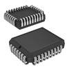
CY7C419-15JXC
Infineon Technologies
IC ASYNC FIFO MEM 256X9 32-PLCC
NCP692MN18T2G
onsemi
IC REG LINEAR 1.8V 1A 6DFN
UPA2211T1M-T1-AT
Renesas Electronics America Inc
MOSFET P-CH 12V 7.5A 8VSOF
0603YC392JAT2A
KYOCERA AVX
CAP CER 3900PF 16V X7R 0603
AT45DB041B-TI
Microchip Technology
IC FLASH 4MBIT SPI 20MHZ 28TSOP
RT1206DRE0790KL
YAGEO
RES SMD 90K OHM 0.5% 1/4W 1206
GRM0335C2A8R9CA01D
Murata Electronics
CAP CER 8.9PF 100V C0G/NP0 0201
06035A3R3C4T2A
KYOCERA AVX
CAP CER 3.3PF 50V NP0 0603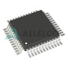
L99PD08
STMicroelectronics
IC PWR DRIVER N-CHAN 1:8 32LQFP
AD9748ACPZRL7
Analog Devices Inc.
IC DAC 8BIT A-OUT 32LFCSP
OZ-SS-124L1
TE Connectivity Potter & Brumfield Relays
RELAY GEN PURPOSE SPDT 16A 24V -

CL21A106KAYNNNE
Samsung Electro-Mechanics
CAP CER 10UF 25V X5R 0805
FWP-50A14FA
Eaton - Bussmann Electrical Division
FUSE CARTRIDGE 50A 700VAC/800VDC
MCP6561RT-E/OT
Microchip Technology
IC COMPARATOR 1 GEN PUR SOT23-5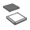
MC13203FC
NXP USA Inc.
IC RF TXRX 802.15.4 32VFQFN
135D685X9125C6
Vishay Sprague
CAP TANT 6.8UF 10% 125V AXIAL
08052U430KAT2A
KYOCERA AVX
CAP CER 43PF 200V NP0 0805
CDBU0230
Comchip Technology
DIODE SCHOTTKY 30V 200MA 0603C
NCP603SNADJT1G
onsemi
IC REG LIN POS ADJ 300MA 5TSOP
MIC5219-3.3BMM
Microchip Technology
IC REG LINEAR 3.3V 500MA 8MSOP
SI501-PROG-CAX
Silicon Labs
MEMS OSC PROG BLANK 32KHZ-100MHZ
MAX232ESE
Analog Devices Inc./Maxim Integrated
RS-232 DRIVER/RECEIVER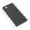
SN74LV10ADR
Texas Instruments
IC GATE NAND 3CH 3-INP 14SOIC
AP7365-30WG-7
Diodes Incorporated
IC REG LINEAR 3V 600MA SOT25
M2S060TS-FGG484I
Microchip Technology
IC SOC CORTEX-M3 166MHZ 484FBGA
DCW03A-12
MEAN WELL USA Inc.
DC DC CONVERTER +/-12V 3W
C4532JB1E106M250KA
TDK Corporation
CAP CER 10UF 25V JB 1812
S9S12VR64AF0MLF
NXP USA Inc.
IC MCU 16BIT 64KB FLASH 48LQFP
ISL6561IRZ
Renesas Electronics America Inc
IC REG CTRLR INTEL 4OUT 40QFN