EP20K100EFC324-1X FPGA: Features, Specifications, Applications, and Programming Guide
The EP20K100EFC324-1X is a programmable chip (FPGA) from Intel’s Altera APEX-20KE® series. It is designed to handle complex digital circuits and supports high-speed data processing. This guide explains its features, specifications, how to program it, and its advantages, making it a helpful resource for everyone.Catalog

EP20K100EFC324-1X Overview
The EP20K100EFC324-1X is part of Intel's Altera APEX-20KE® series, a Field Programmable Gate Array (FPGA) tailored for high-density programmable logic applications that necessitate sophisticated system-on-a-programmable-chip (SOPC) integrations. This device is distinguished by its integration of 4,160 logic elements or cells and 416 Logic Array Blocks (LABs), which facilitate substantial configurability for various digital circuit designs. It also boasts a considerable amount of embedded memory accommodating demanding data storage requirements within the FPGA. Further enhancing its application versatility, the EP20K100EFC324-1X supports 246 I/O pins and offers a substantial gate count of approximately 263,000 equivalent gates, operating efficiently between 1.71V to 1.89V. It is packaged in a 324-ball Fine-Pitch Ball Grid Array (FBGA), which aids in robust physical integration into electronic assemblies.
The EP20K100EFC324-1X is the perfect choice when you’re ready to place bulk orders with us for your projects or product lines.
EP20K100EFC324-1X CAD Models
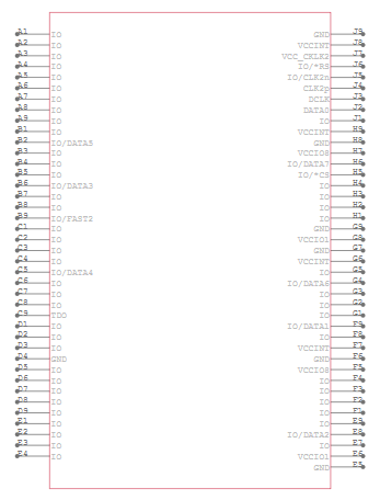
EP20K100EFC324-1X Symbol
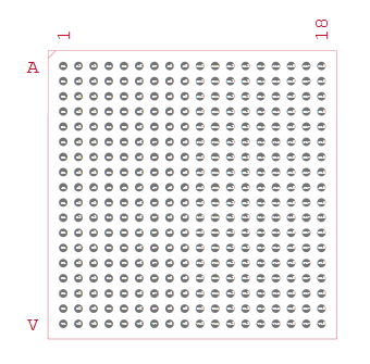
EP20K100EFC324-1X Footprint
EP20K100EFC324-1X 3D Model
EP20K100EFC324-1X Features
• High Logic Density: The FPGA is equipped with 4,160 logic elements (LEs) and 416 Logic Array Blocks (LABs). This high density of logic cells allows for the design and execution of complex digital circuits and systems within a single chip, making it ideal for applications requiring robust logic processing capabilities.
• Embedded Memory: Offering 53,248 RAM bits, this FPGA provides substantial embedded memory resources. This feature is good for applications that require fast data storage and retrieval, allowing for efficient handling of data-intensive tasks.
• Extensive I/O Capabilities: With 246 input/output pins, the EP20K100EFC324-1X ensures comprehensive connectivity and interfacing options. This broad range of I/O capabilities enables it to easily connect with a multitude of external devices and systems, enhancing its utility in complex electronic assemblies.
• Multi-Voltage Support: The device supports a core voltage range of 1.71V to 1.89V and features MultiVolt™ I/O interfacing. This allows the FPGA to be compatible with other electronic components that operate at various logic levels, including 1.8V, 2.5V, 3.3V, and 5.0V, providing great flexibility in system design.
EP20K100EFC324-1X Block Diagram
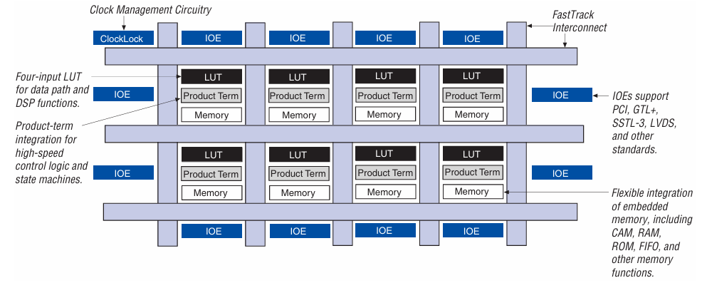
The EP20K100EFC324-1X block diagram represents the internal structure of an FPGA (Field Programmable Gate Array) device, showcasing its various functional units. The diagram consists of interconnected logic blocks, memory elements, clock management, and I/O elements. At the core of the design are Logic Array Blocks (LABs), which contain Look-Up Tables (LUTs) and product-term-based logic. These elements allow flexible logic implementation, making the FPGA suitable for high-speed control logic, state machines, and DSP functions. The FastTrack Interconnect provides a high-speed communication pathway between logic elements, ensuring efficient signal routing throughout the device. The Clock Management Circuitry, including the ClockLock feature, ensures reliable and synchronized operation by stabilizing and distributing clock signals across the FPGA. The Input/Output Elements (IOEs), positioned around the FPGA fabric, serve as interfaces for external communication. These IOEs support multiple industry-standard protocols such as PCI, GTL+, SSTL-3, and LVDS, enabling the FPGA to interface with a variety of external systems. These IOEs ensure compatibility with different voltage levels and signaling standards, enhancing the FPGA’s versatility in embedded applications. Embedded memory blocks provide flexible storage solutions within the FPGA. These memory elements can function as Content Addressable Memory (CAM), Random Access Memory (RAM), Read-Only Memory (ROM), First-In-First-Out (FIFO) buffers, and other memory structures. The ability to integrate memory directly within the FPGA fabric improves data processing efficiency, reducing external memory dependencies and latency.
EP20K100EFC324-1X Specifications
|
Type |
Parameter |
|
Manufacturer |
Intel |
|
Series |
APEX-20KE® |
|
Packaging |
Tray |
|
Part Status |
Obsolete |
|
Number of LABs/CLBs |
416 |
|
Number of Logic Elements/Cells |
4160 |
|
Total RAM Bits |
53248 |
|
Number of I/O |
246 |
|
Number of Gates |
263000 |
|
Voltage - Supply |
1.71V ~ 1.89V |
|
Mounting Type |
Surface Mount |
|
Operating Temperature |
0°C ~ 85°C (TJ) |
|
Package / Case |
324-BGA |
|
Supplier Device Package |
324-FBGA (19x19) |
|
Base Product Number |
EP20K100 |
EP20K100EFC324-1X Applications
Networking and Communications
This FPGA is ideal for networking equipment such as routers and switches, where it manages data routing, signal processing, and protocol handling. Its high logic density and extensive I/O capabilities allow it to support the complex, high-speed data operations required in modern communications infrastructure.
Industrial Control Systems
In the industrial sector, the EP20K100EFC324-1X excels in automation systems. Its programmability and robust processing capabilities enable precise control and monitoring for enhancing operational efficiency and reliability in manufacturing processes.
Automotive Electronics
The FPGA serves as a component in automotive applications, particularly in advanced driver-assistance systems (ADAS) and in-vehicle infotainment systems. It provides the necessary processing power and adaptability to handle data and support the sophisticated functionalities required in modern vehicles.
Consumer Electronics
Due to its flexibility and high performance, the EP20K100EFC324-1X is also found in consumer electronics like high-definition televisions and gaming consoles. It supports complex functionalities and aids in shortening product development cycles, meeting the fast-paced demand of the consumer electronics market.
Medical Devices
In the medical field, this FPGA contributes to the functionality of medical imaging equipment and diagnostic tools. Its ability to process data at high speeds ensures that these devices can deliver accurate and timely diagnostic results for effective medical treatment and imaging.
EP20K100EFC324-1X Similar Parts
EP20K100EFC324-1X Programming Steps
To effectively program the EP20K100EFC324-1X, a member of Altera's APEX-20KE® FPGA series, it's important to follow a structured sequence of steps. This process ensures that your design is efficiently translated into a format that the FPGA can execute. Below, I outline a detailed approach to programming this FPGA model, integrating steps and modifications specific to this device.
1. Design Entry
Begin by creating your digital logic design. Utilize hardware description languages (HDLs) such as VHDL or Verilog, which allow you to describe the hardware functionality and logic of your system. Tools like Altera's Quartus II offer a comprehensive environment for writing, testing, and compiling your HDL code. Ensure that your design is modular, making it easier to debug and scale.
2. Synthesis
Once your design entry is complete, the next step is synthesis, where the HDL code is translated into a netlist. This netlist represents the interconnected list of gates, flip-flops, and other hardware elements that make up your design. During synthesis, the code is optimized for the specific architecture of the EP20K100EFC324-1X, ensuring that the design utilizes the FPGA's resources effectively. Tools like Synplify Pro or the synthesis tool within Quartus II can be used for this purpose. It's important to focus on optimizing your design to meet timing and resource constraints.
3. Implementation
Following synthesis, implementation takes place. This step involves mapping the netlist to the actual FPGA hardware. It includes the placement of the logic elements within the FPGA and the routing of the connections between them. The Quartus II software facilitates this process through its implementation tools, which manage the placement and routing to meet the desired clock speeds and performance metrics. During implementation, you may need to iterate on your design based on the feedback from timing analysis tools to ensure that all performance requirements are met.
4. Bitstream Generation
After successful implementation, the next phase is generating the bitstream. This is the binary file that will be loaded onto the FPGA. The bitstream contains configured data for every programmable element in the FPGA, setting up the device to perform the functions as per your design. The Quartus II software can generate this bitstream, which is then ready to be downloaded to the FPGA.
5. Programming the FPGA
The final step is to program the FPGA with the generated bitstream. This can be done using a hardware programmer compatible with the EP20K100EFC324-1X, such as the USB Blaster. Connect the programmer to your development board where the FPGA is mounted and use the Quartus II Programmer tool to transfer the bitstream to the FPGA. This step will load your design onto the FPGA, and it will begin to operate according to the logic defined in your HDL code.
EP20K100EFC324-1X Advantages
High Integration
The EP20K100EFC324-1X offers high integration capabilities due to its large number of logic elements and embedded memory. This integration allows for the consolidation of multiple functionalities into a single device. As a result, systems can be simplified, reducing the overall component count, physical space required, and potential points of failure in electronic designs.
Flexible Logic Implementation
The architecture of the EP20K100EFC324-1X supports both look-up table (LUT) and product-term-based logic. This flexibility in logic implementation enables to optimize the FPGA for a wide range of applications, from simple logic gates to complex combinational circuits. It provides an advantage in terms of design versatility and can accommodate a broad spectrum of digital functionalities.
Advanced Interconnect Structure
Featuring a hierarchical interconnect structure, the FPGA includes local, MegaLAB™, and FastTrack® interconnections. These specialized routing resources enhance signal routing efficiency and improve the overall performance of the device. This advanced interconnect structure is good for designs that require high-speed data transmission and low latency, making the FPGA ideal for high-performance computing and telecommunications.
Clock Management
The EP20K100EFC324-1X incorporates ClockLock and ClockBoost technology, which aids in effective clock management. These features help in maintaining the integrity of the clock signal throughout the FPGA, reducing jitter and improving signal reliability. Effective clock management is needed for synchronous digital circuits, ensuring stable and predictable operation across various environmental conditions.
Design Flexibility
The programmable nature of the EP20K100EFC324-1X allows to tailor hardware to specific needs and reconfigure the FPGA for different applications or updates. This flexibility means that a single FPGA can be used across multiple projects, which is beneficial in a dynamic technological landscape where requirements can change rapidly.
Rapid Prototyping
FPGAs like the EP20K100EFC324-1X enable rapid prototyping of digital circuits. You can develop and iterate designs quickly without the lengthy lead times associated with custom ASIC development. This ability to quickly model and test new designs accelerates the development process, leading to faster innovation and shortened time-to-market.
Cost Efficiency
Integrating multiple functions within a single FPGA reduces the need for additional discrete components, which can lead to cost savings in both procurement and assembly. This integration also simplifies the manufacturing process and can reduce the overall system complexity, leading to lower maintenance and upgrade costs over the product’s lifecycle.
Long-Term Support
The reconfigurable aspect of the EP20K100EFC324-1X ensures that hardware can be updated to fix bugs, improve performance, or add new features without requiring physical hardware changes. This long-term support and adaptability protect investments and enable devices to stay relevant as new standards and technologies emerge.
EP20K100EFC324-1X Packaging Dimensions
The EP20K100EFC324-1X is an FPGA from Altera's APEX-20KE® series, housed in a 324-ball Fine-Pitch Ball Grid Array (FBGA) package. Its packaging dimensions are as follows:
• Pitch: 1 mm
• Length × Width: 19 mm × 19 mm
• Area: 361 mm²
EP20K100EFC324-1X Manufacturer
The EP20K100EFC324-1X is a model from the APEX-20KE® series of Field Programmable Gate Arrays (FPGAs) originally developed by Altera. After Intel's acquisition of Altera in 2015, this FPGA and other Altera products became part of Intel's extensive programmable solutions portfolio. As a result, Intel continues to support Altera's product lines while integrating them with their own advanced technology offerings. Although the EP20K100EFC324-1X has been classified as obsolete and is no longer in production, its legacy is maintained under Intel, which recommends newer FPGA models for current applications to ensure long-term support and availability.
Conclusion
The EP20K100EFC324-1X is a powerful and flexible FPGA that allows to create and test custom digital circuits. It offers high performance, built-in memory, and multi-voltage support, making it useful in many industries. This guide has taken you through the main features, design, and steps to program this FPGA in a simple way, so you can easily understand and use it.
Datasheet PDF
EP20K100EFC324-1X Datasheets:
About us
ALLELCO LIMITED
Read more
Quick inquiry
Please send an inquiry, we will respond immediately.
Frequently Asked Questions [FAQ]
1. How does the EP20K100EFC324-1X compare to newer FPGA models?
The EP20K100EFC324-1X remains a powerful FPGA for legacy systems and industrial applications that require high logic density and flexible I/O capabilities. However, compared to modern FPGAs like Intel's Cyclone, Arria, or Stratix series, it lacks advanced power efficiency, high-speed transceivers, and AI-driven acceleration. If you're designing a new system, we can suggest equivalent or upgraded models.
2. Does the EP20K100EFC324-1X support external memory interfaces like DDR or SRAM?
Yes, the EP20K100EFC324-1X supports external memory interfaces, including SRAM and SDRAM. However, it does not natively support DDR2/DDR3. If high-speed memory interfacing is required, additional external logic or a newer FPGA might be necessary.
3. Can I reconfigure the EP20K100EFC324-1X multiple times?
Yes, like all FPGAs, this device is fully reprogrammable. However, if using a volatile configuration, you will need an external memory (such as a serial PROM) to retain the design after power cycling.
4. Can I program the EP20K100EFC324-1X using Intel Quartus software?
Yes, you can program the EP20K100EFC324-1X using Intel Quartus II (legacy versions), as this FPGA belongs to the APEX-20KE® family. Ensure that your Quartus II version supports this device, as newer Quartus Prime editions do not support legacy FPGAs.
5. What power supply requirements should I consider when using the EP20K100EFC324-1X?
The EP20K100EFC324-1X operates with a core voltage range of 1.71V to 1.89V. It also features MultiVolt™ I/O technology, supporting 1.8V, 2.5V, 3.3V, and 5.0V logic levels. Ensure that your power supply meets these voltage requirements for stable performance.

XCV200-6FG456C FPGA: Features, Specifications, Programming, and Applications
on March 20th

Why 0603 Components Are Popular in Modern Electronics
on March 20th
Popular Posts
-

Complex Instruction Set Computers: How They Changed Computing?
on April 18th 147765
-

USB-C Pinout and Features
on April 18th 111994
-

Using Xilinx Unified Simulation Primitives: A Comprehensive Guide to FPGA Design and Simulation
on April 18th 111351
-

Power Supply Voltages in Electronics: Meaning of VCC, VDD, VEE, VSS, and GND
on April 18th 83753
-

RJ45 Connector Guide: Pinout, Wiring, Cable Types, and Uses
on January 1th 79548
-

The Ultimate Guide to Wire Color Codes in Modern Electrical Systems
The way our electrical systems use colors isn’t just for looks. Each wire color now indicates a specific function, making it easier to identify and handle electrical components correctly during ins...on January 1th 66949
-

Purge Valve Guide: Function, Symptoms, Testing, and Replacement for Optimal Engine Performance
The purge valve is a key part of a car’s system that helps keep the air clean by managing fuel vapors before they can escape into the atmosphere. This not only helps the environment by reducing pol...on January 1th 63094
-

Quality (Q) Factor: Equations and Applications
The quality factor, or 'Q', is important when checking how well inductors and resonators work in electronic systems that use radio frequencies (RF). 'Q' measures how well a circuit minimizes energy...on January 1th 63028
-

Achieving Peak Performance with the Maximum Power Transfer Theorem
The Maximum Power Transfer Theorem explains how energy from a source, such as a battery or generator, flows to a connected load. It shows the exact condition where the load receives the most power....on January 1th 54094
-

A23 Battery Specifications and Compatibility
The A23 battery is a small, cylinder-shaped battery with high voltage. Also called 23A, 23AE, or MN21, it runs at 12 volts and much higher than AA or AAA batteries. Its special design make...on January 1th 52175
HOT Part Number
-

SP6205EM5-L/TR
MaxLinear, Inc.
IC REG LIN POS ADJ 500MA SOT23-5
MAX6163AESA+T
Analog Devices Inc./Maxim Integrated
IC VREF SERIES 0.07% 8SOIC
BM06B-XASS-TF
JST Sales America Inc.
CONN HEADER SMD 6POS 2.5MM
ADS7861E
Texas Instruments
IC ADC 12BIT SAR 24SSOP
AD8605ACB-REEL7
Analog Devices Inc.
IC OPAMP GP R-R CMOS PREC 5WLCSP
GRM2165C2A121JA01D
Murata Electronics
CAP CER 120PF 100V C0G/NP0 0805
AD7576JN
Analog Devices Inc.
8-BIT SAR ADC, PARALLEL ACCESS
1N5386BG
onsemi
DIODE ZENER 180V 5W AXIAL
FAN1655M
onsemi
IC REG CTRLR DDR 1OUT 14SOIC
JW100H1
ABB Power Electronics Inc.
DC DC CONVERTER 24V 100W
EMH2412-TL-H
Sanyo
N-CHANNEL MOSFET
PIC16F818T-I/SO
Microchip Technology
IC MCU 8BIT 1.75KB FLASH 18SOIC
CD4030BPWR
Texas Instruments
IC GATE XOR 4CH 2-INP 14TSSOP
AD7175-8BCPZ-RL
Analog Devices Inc.
IC ADC 24BIT SIGMA-DELTA 40LFCSP
TH72032KDC-BAA-000-RE
Melexis Technologies NV
RF XMITTER ASK 868/915MHZ 8SOIC
T520V227M006ATE040
KEMET
CAP TANT POLY 220UF 6.3V 2917
NVD14N03RT4G
onsemi
N-CHANNEL POWER MOSFET
RT0805DRD0751KL
YAGEO
RES SMD 51K OHM 0.5% 1/8W 0805 -
LTC2229IUH#PBF
Analog Devices Inc.
IC ADC 12BIT PIPELINED 32QFN
BC856A
Taiwan Semiconductor Corporation
SOT-23, -80V, -0.1A, PNP BIPOLAR
74ACT574
AMI Semiconductor / ON Semiconductor
IC FF D-TYPE SNGL 8BIT DIE
A4949GLJTR-T
Allegro MicroSystems
IC FAN DRIVER BLDC 8SOIC
SD417+
Analog Devices Inc./Maxim Integrated
MODULE INTERFACE SENSOR
BQ24032RHLR
Texas Instruments
IC BATT CHG LI-ION 1CELL 20VQFN
SMBJ8.5A
Meritek
TVS DIODE 8.5VWM 14.4VC
W25Q256JVFJM
Winbond Electronics
IC FLASH 256MBIT SPI/QUAD 16SOIC
IPP086N10N3
Infineon Technologies
N-CHANNEL POWER MOSFET
TNY266PN
Power Integrations
IC OFFLINE SWITCH FLYBACK 8DIP
X9511WS
Intersil
DIGIPOT, 32 POSITIONS
GRM1555C1E7R4CZ01D
Murata Electronics
CAP CER 7.4PF 25V C0G/NP0 0402
XC6218P302HR-G
Torex Semiconductor Ltd
IC REG LINEAR 3V 200MA 3USP
HI5812JIP
Renesas Electronics America Inc
IC ADC 12BIT SAR 24DIP
MCIMX503CVM8B
NXP USA Inc.
IC MPU I.MX50 800MHZ 400MAPBGA
281742-5
TE Connectivity AMP Connectors
CONN HEADER R/A 10POS 2.54MM
RT1206DRD0724KL
YAGEO
RES SMD 24K OHM 0.5% 1/4W 1206
KSZ8041NL-TR
Microchip Technology
IC TRANSCEIVER FULL 1/1 32MLF -
MAX802MCSA+
Analog Devices Inc./Maxim Integrated
IC SUPERVISOR 1 CHANNEL 8SOIC
MCP1811AT-033/OT
Microchip Technology
IC REG LINEAR 3.3V 150MA SOT23-5
MIC5355-SGYMME
Microchip Technology
IC REG LINEAR 1.8V/3.3V 8MSOP
08051A151GA12A
KYOCERA AVX
CAP CER 150PF 100V NP0 0805
MC33772BSP1AE
NXP USA Inc.
IC BATT CNTRL LI-ION 3-6C 48LQFP
MAX3964AETP
Analog Devices Inc./Maxim Integrated
IC LIMITING AMP 20TQFN
KSP43TA
onsemi
TRANS NPN 200V 0.5A TO92-3
ADM3485EAN
Analog Devices Inc.
IC TXRX RS-485 HS 3.3V 8DIP
GRM0225C1C6R8DD05L
Murata Electronics
CAP CER 6.8PF 16V C0G/NP0 01005
C1608Y5V1C105Z/10
TDK Corporation
CAP CER 1UF 16V Y5V 0603
P6KE110CA
SMC Diode Solutions
TVS DIODE 94VWM 152VC DO15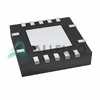
AR2003FV-13
Diodes Incorporated
IC RECT CTRLR ACT/SYNC 14VDFN
744761156C
Würth Elektronik
FIXED IND 56NH 600MA 250MOHM SMD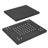
MT29F4G08ABADAH4-IT:D
Micron Technology Inc.
IC FLASH 4GBIT PARALLEL 63VFBGA
MP2012DQ-LF-Z
Monolithic Power Systems Inc.
IC REG BUCK ADJUSTABLE 1.5A 6QFN
SN74AHC04NSR
Texas Instruments
IC INVERTER 6CH 1-INP 14SOP
PIC16C54C-20I/SS
Microchip Technology
IC MCU 8BIT 768B OTP 20SSOP
MJE371
onsemi
TRANS PNP 40V 4A TO126