XCV200-6FG456C FPGA: Features, Specifications, Programming, and Applications
The XCV200-6FG456C is a powerful FPGA (Field-Programmable Gate Array) from the AMD Xilinx Virtex® series. This guide explains its features, pin layout, programming steps, and uses. With high processing power, flexible design options, and strong input/output (I/O) capabilities, this FPGA helps build fast and reliable digital systems. Whether you’re working on networking, control systems, or custom electronics, this guide will help you understand how the XCV200-6FG456C can be used in your projects.Catalog

XCV200-6FG456C Overview
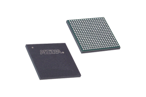
The XCV200-6FG456C is a notable model within the AMD Xilinx Virtex® FPGA family, designed to provide robust programmable logic solutions for complex digital systems. This specific chip encompasses approximately 236,666 system gates and features 1,176 Configurable Logic Blocks (CLBs) and 5,292 logic cells. It also includes 57,344 total RAM bits and supports 284 I/O pins, housed in a 456-ball Fine-Pitch Ball Grid Array (FBGA) package, measuring 23mm x 23mm. This model operates on a 2.5V nominal voltage, with a range of 2.375V to 2.625V, and can function within a temperature range of 0°C to 85°C. The broader Virtex® series caters to a range of applications with densities from 50,000 to over 1 million system gates and system clock rates of up to 200 MHz. It supports numerous I/O standards including LVTTL, LVCMOS, and PCI, among others. Features such as Delay-Locked Loops (DLLs), configurable logic blocks with embedded memory, and dedicated carry logic for arithmetic operations enhance its functionality. Manufactured using a 0.22 µm 5-layer metal process, the Virtex® family guarantees performance and reliability.
If you're looking to integrate top-tier FPGA technology into your products or systems, buying the XCV200-6FG456C in bulk with us is a smart move. It meets industry standards and keeps you ahead of future technology needs.
XCV200-6FG456C Features
• System Gates: The XCV200-6FG456C offers approximately 236,666 system gates. This high gate count allows for the implementation of complex integrated digital logic circuits on a single chip, enhancing both performance and versatility in a range of applications.
• Logic Resources: It includes 1,176 Configurable Logic Blocks (CLBs) and 5,292 logic cells. These resources are good for designing flexible and scalable digital circuits. CLBs can be programmed to perform a wide variety of logical functions, while the large number of logic cells enables the handling of extensive logic operations and processes.
• Memory: The device provides 57,344 bits of RAM, distributed among its logic blocks. This embedded RAM is used for applications that require fast and efficient data storage and retrieval, supporting high-speed data operations integral to modern digital systems.
• I/O Capabilities: With 284 Input/Output pins, the XCV200-6FG456C facilitates extensive interfacing capabilities. These I/O pins support various signal standards and enable the FPGA to communicate effectively with other components in a system, such as memory devices, processors, and peripherals.
• Voltage and Temperature Range: Operating at a nominal voltage of 2.5V, with an acceptable range from 2.375V to 2.625V, this FPGA is designed for low-power consumption while maintaining robust performance. It can operate within a junction temperature range of 0°C to 85°C, ensuring reliability under varying environmental conditions.
XCV200-6FG456C Pin Function Diagram
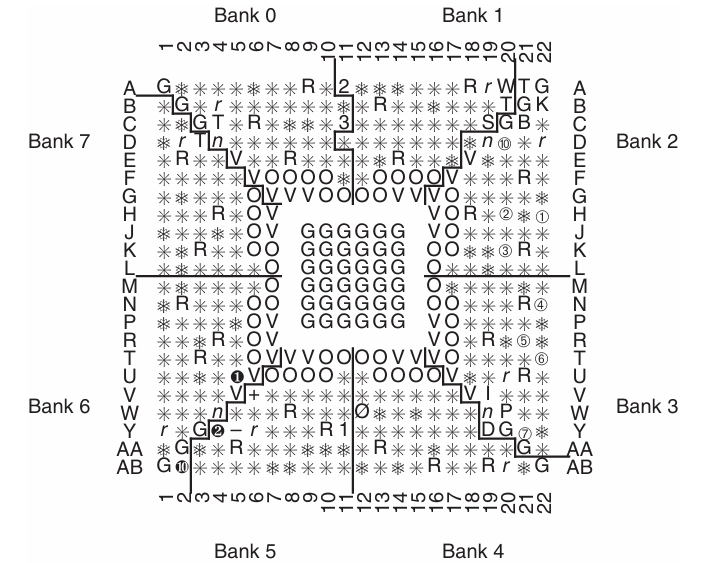
The XCV200-6FG456C pin function diagram is a structured representation of the FPGA’s pin assignments, categorized into different banks (Bank 0 to Bank 7). Each bank groups pins based on their function and physical placement on the FPGA package. The numbering and labeling system follows a grid pattern where rows are denoted by letters (A, B, C, etc.), and columns by numbers (1, 2, 3, etc.), which facilitates quick identification of specific pins. These banks correspond to different input/output functions, power, ground, and dedicated signal routing. Pins are assigned various functional groupings, including General-Purpose I/O (GPIO), often labeled as "G" (General Input/Output), "V" (Voltage supply), and "O" (Output). Power and ground pins are marked distinctly, ensuring stable FPGA operation. Special-purpose pins such as clock inputs, resets, and control signals are identified with symbols like "R" or "T." Some pins also serve dedicated communication roles, including JTAG configuration and high-speed clocking, for programming and debugging.
XCV200-6FG456C Block Diagram
Input/Output Block
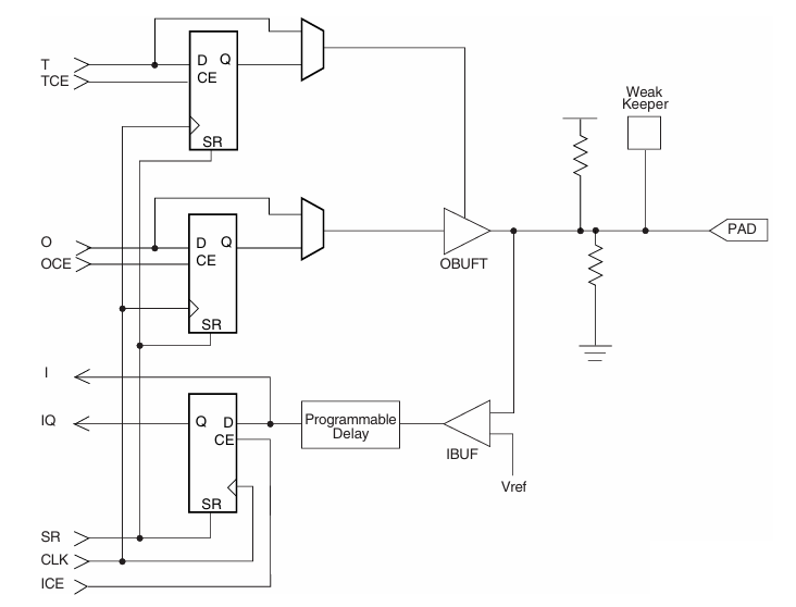
The diagram represents the Input/Output Block (IOB) structure of the XCV200-6FG456C FPGA, which is a member of the Xilinx Virtex family. The diagram showcases key elements involved in input and output operations, highlighting the data flow and control mechanisms. At the core of the diagram, three D flip-flops are used to register signals for input, output, and tri-state control. The output register is controlled by the OCE (Output Clock Enable) signal, which determines when the output data is latched. Similarly, the tri-state register is controlled by the TCE (Tri-State Clock Enable), enabling or disabling the output buffer. The input register captures incoming data and applies a programmable delay before passing it to the internal FPGA logic through the IBUF (Input Buffer). The OBUFT (Tri-State Output Buffer) ensures that the FPGA can either drive a signal onto the PAD (I/O pin) or place it in a high-impedance state, depending on the control logic. A weak keeper circuit is included on the PAD to maintain the last known logic state when no active driver is present, preventing unintended floating conditions. The reference voltage (Vref) is used for certain input standards, such as SSTL or HSTL, which require precise voltage levels for proper operation. Overall, this IOB structure allows the FPGA to manage high-speed data transmission, support different I/O standards, and provide flexible control over signal timing and integrity.
Master/Slave Serial Mode
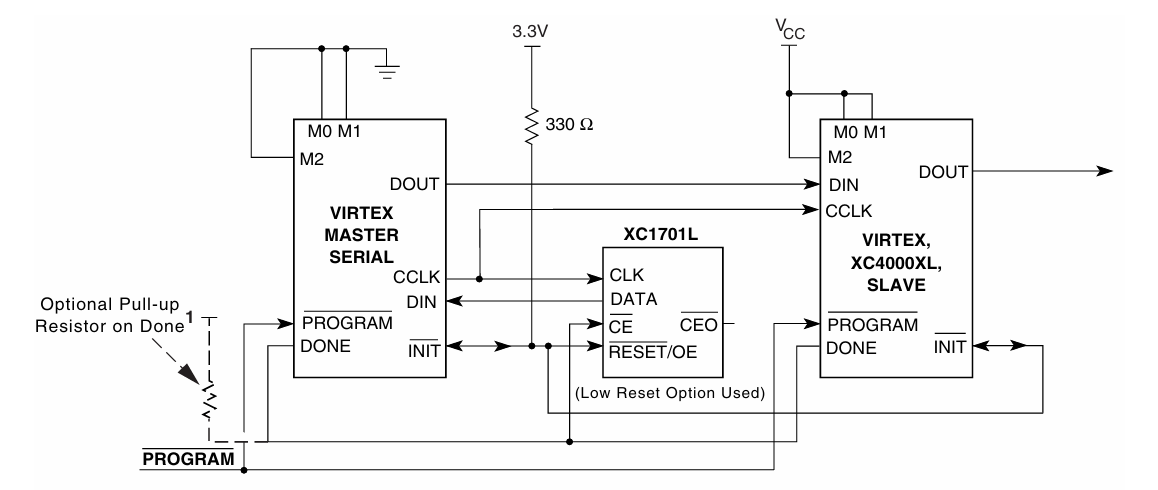
The Master/Slave Serial Mode block diagram illustrates the configuration process of a Virtex FPGA, specifically the XCV200-6FG456C, when programmed in a daisy-chain configuration using a serial EEPROM (XC1701L). In this setup, one Virtex device operates as the Master, controlling the configuration clock (CCLK) and serially transmitting configuration data to additional Slave FPGAs in the chain. The Master FPGA initiates the configuration process by asserting the PROGRAM signal, resetting all devices in the chain. Once initialization is complete, the INIT signal indicates readiness, and configuration data flows from the serial EEPROM (XC1701L) to the DIN (Data In) pin of the Master FPGA. The Master FPGA reads data from the EEPROM and forwards it through DOUT (Data Out) to subsequent Slave FPGAs, synchronizing data transfer using the CCLK signal. The DONE signal is used to indicate successful configuration, with an optional pull-up resistor ensuring a stable high state when configuration is complete. The XC1701L EEPROM is controlled by the Master FPGA using CLK, DATA, CE (Chip Enable), and RESET/OE (Output Enable) signals, ensuring that the stored configuration data is correctly retrieved. This configuration method is efficient for programming multiple FPGAs using a single EEPROM, reducing external wiring complexity and ensuring all devices receive synchronized configuration data.
XCV200-6FG456C Specifications
|
Type |
Parameter |
|
Manufacturer |
AMD Xilinx |
|
Series |
Virtex® |
|
Packaging |
Tray |
|
Part Status |
Obsolete |
|
Number of LABs/CLBs |
1176 |
|
Number of Logic Elements/Cells |
5292 |
|
Total RAM Bits |
57344 |
|
Number of I/O |
284 |
|
Number of Gates |
236666 |
|
Voltage - Supply |
2.375V ~ 2.625V |
|
Mounting Type |
Surface Mount |
|
Operating Temperature |
0°C ~ 85°C (TJ) |
|
Package / Case |
456-BBGA |
|
Supplier Device Package |
456-FBGA (23x23) |
|
Base Product Number |
XCV200 |
XCV200-6FG456C Applications
Telecommunications and Networking
The XCV200-6FG456C excels in telecommunications and networking applications due to its ability to handle high-speed data transmissions and complex signal processing tasks. Its high gate count and robust I/O capabilities allow it to support functions such as packet processing, signal modulation/demodulation, and error correction protocols.
Digital Signal Processing (DSP)
Ideal for DSP applications, this FPGA can perform rapid and complex mathematical computations required in audio and video processing technologies. Whether it's for multimedia systems, voice recognition, or streaming services, the XCV200-6FG456C's powerful processing capabilities and embedded memory support efficient and high-quality signal processing.
Industrial Control Systems
In the industrial automation, the XCV200-6FG456C provides the necessary performance to manage control systems and automation networks. Its ability to execute multiple control tasks simultaneously while ensuring response times makes it suitable for applications in process control, robotics, and machine vision.
Medical Instruments
The FPGA's precision and speed are great in medical imaging and diagnostic equipment, where it aids in the processing of complex algorithms for imaging applications such as MRI, ultrasound, and CT scans. The XCV200-6FG456C's capabilities ensure that it can handle high data throughput and intricate processing required in modern medical technology.
XCV200-6FG456C Similar Parts
XCV200-6FG456C Programming Steps
Programming Steps for the XCV200-6FG456C:
1. Design Entry
The initial phase of FPGA programming involves defining the digital logic and functionality of your system. This can be done using Hardware Description Languages (HDLs) such as VHDL or Verilog, where you write code that specifies how the FPGA processes data and interacts with other hardware. Schematic entry tools available in FPGA design software like Xilinx ISE or Vivado can be utilized. This method involves creating a visual representation of the logic by dragging and dropping components, which some find more intuitive than writing code.
2. Synthesis
Once the design is completed, the next step is synthesis, where a tool like Xilinx's XST (Xilinx Synthesis Technology) transforms your HDL code or schematic design into a netlist. This netlist describes the circuit in terms of generic digital components, such as logic gates and registers. The synthesis process also involves optimizing the design to meet performance requirements and minimize resource usage for efficient FPGA operation.
3. Implementation
The implementation process begins with translation, combining your design with constraint files that specify parameters such as clock frequencies and pin assignments. Following translation, the mapping stage assigns the elements of your netlist to specific physical resources on the FPGA, like Look-Up Tables (LUTs) and flip-flops. The placement and routing phase then determines the physical locations of each component within the FPGA's architecture and establishes the connections between them through programmable interconnect resources. This stage is great for achieving the desired performance metrics, including clock frequencies.
4. Bitstream Generation
After successful placement and routing, the tool generates a bitstream, a binary configuration file that contains all the programming information for the FPGA. It is often recommended to simulate the final design post-placement to ensure the bitstream will behave as expected under conditions. This verification step helps to avoid potential issues during actual operation.
5. Configuration
The final step involves loading the bitstream into the FPGA using various configuration methods. The slave-serial mode, a simple and cost-effective option, configures the FPGA via an external master device that sends data serially. In master-serial mode, the FPGA autonomously reads the bitstream from an attached serial PROM. For high-speed configurations, SelectMAP mode allows an external microprocessor to load data into the FPGA quickly. Additionally, JTAG mode is used not only for programming but also for testing and debugging, utilizing a standard interface for in-system programming and boundary-scan testing.
XCV200-6FG456C Advantages
Performance
The Xilinx Virtex series, to which the XCV200-6FG456C belongs, is optimized for high-speed performance, offering system clock rates of up to 200 MHz. This makes it well-suited for applications that require fast data processing, ensuring efficient handling of complex algorithms and high-speed operations like telecommunications, processing, and multimedia.
I/O Standards Support
This FPGA supports a wide range of Input/Output standards, including LVTTL, LVCMOS, PCI, GTL, HSTL, SSTL, CTT, and AGP. Such extensive I/O standards support enables the XCV200-6FG456C to integrate seamlessly with various system components, enhancing its utility across diverse digital ecosystems. This flexibility allows to adapt the FPGA to different interfacing conditions without system modifications.
Clock Management
The XCV200-6FG456C incorporates multiple Delay-Locked Loops (DLLs) for clock distribution and management within the system. These DLLs help in improving system timing and reliability by providing precise clock signals necessary for synchronous operations. This feature is important in reducing system errors and enhancing overall performance, particularly in complex designs requiring accurate timing and synchronization.
Design Flexibility
With 1,176 Configurable Logic Blocks and 5,292 logic cells, the XCV200-6FG456C offers substantial logic resources with the capability to implement a diverse range of functionalities. From simple glue logic to intricate digital systems, this FPGA supports complex design requirements, making it ideal for applications in custom computing, digital signal processing, and prototyping.
Rapid Prototyping
FPGAs like the XCV200-6FG456C are renowned for their capability to support rapid prototyping. This device allows for quick design iterations and can be reconfigured in-field, which is an advantage for development cycles as it reduces time-to-market. It also adapts efficiently to changing requirements or updates in project specifications, ensuring that the final products are up-to-date with the latest technological standards.
Integration Capability
The integration capabilities of the XCV200-6FG456C facilitate the consolidation of multiple discrete components into a single chip. This integration can lead to reduced system complexity, lower power consumption, and cost savings. By minimizing the number of separate components needed, this FPGA simplifies design processes and improves the reliability and compactness of the overall system.
XCV200-6FG456C Packaging Dimensions
The XCV200-6FG456C is a Field Programmable Gate Array (FPGA) from AMD's Virtex® series, housed in a 456-ball Fine-Pitch Ball Grid Array (FBGA) package.
• Package Type: 456-FBGA
• Package Size: 23 mm x 23 mm
• Ball Pitch: 1.0 mm
XCV200-6FG456C Manufacturer
The XCV200-6FG456C is a Field Programmable Gate Array (FPGA) originally developed by Xilinx, a company known for its high-performance programmable logic devices. Following Xilinx's acquisition by AMD, the XCV200-6FG456C is now associated with AMD as its current manufacturer. However, this FPGA model is obsolete and no longer in production. AMD continues to support newer FPGA architectures with enhanced performance, power efficiency, and extended longevity, making modern alternatives preferable for new designs.
Conclusion
The XCV200-6FG456C is a versatile and high-speed FPGA, useful for many technology applications. While it is no longer being made, it is still a good choice for older systems that need reliable performance. This guide has covered its design, programming steps, and practical uses, making it easier to understand how it works and how it can be used. As newer FPGAs become available, you can use this knowledge to choose the right FPGA for your needs and improve digital designs.
Datasheet PDF
XCV200-6FG456C Datasheets:
About us
ALLELCO LIMITED
Read more
Quick inquiry
Please send an inquiry, we will respond immediately.
Frequently Asked Questions [FAQ]
1. What is the power consumption of the XCV200-6FG456C?
The XCV200-6FG456C operates at 2.5V, with a voltage range of 2.375V to 2.625V. Power consumption depends on logic utilization and clock frequency, but as an older FPGA, it may be less power-efficient than newer Xilinx devices. Proper power management and heat dissipation should be considered.
2. How does the XCV200-6FG456C compare to the XCV200-6FG256C?
The XCV200-6FG456C has a larger package (456-ball FBGA) compared to the XCV200-6FG256C (256-ball FBGA), offering more I/O pins (284 vs. 172) and potentially better performance for applications requiring extensive interfacing. If your design relies on more I/O capabilities, the XCV200-6FG456C is the better choice.
3. Can I reprogram the XCV200-6FG456C multiple times?
Yes, the XCV200-6FG456C is a SRAM-based FPGA, meaning it can be reprogrammed an unlimited number of times as long as power is supplied. However, you will need external non-volatile memory (EEPROM or Flash) to retain the bitstream after a power cycle.
4. Does the XCV200-6FG456C support high-speed serial communication?
The XCV200-6FG456C supports multiple I/O standards such as LVTTL, LVCMOS, PCI, GTL, HSTL, and SSTL, but it does not have built-in high-speed SerDes (Serializer/Deserializer) or transceivers like modern FPGAs. For applications requiring high-speed serial links (e.g., PCIe, Gigabit Ethernet, or HDMI), consider newer FPGA models.
5. How does the XCV200-6FG456C compare to newer FPGA models?
The XCV200-6FG456C belongs to an older generation of FPGAs. Compared to modern Virtex FPGAs, it has a lower gate count, slower clock speeds, and limited power efficiency. Newer models offer higher logic density, more embedded memory, advanced DSP blocks, and lower power consumption, making them better for modern applications.
AD73322AR Pinout, Features, and Technical Details Explained
on March 21th
EP20K100EFC324-1X FPGA: Features, Specifications, Applications, and Programming Guide
on March 20th
Popular Posts
-

Complex Instruction Set Computers: How They Changed Computing?
on April 18th 147760
-

USB-C Pinout and Features
on April 18th 111967
-

Using Xilinx Unified Simulation Primitives: A Comprehensive Guide to FPGA Design and Simulation
on April 18th 111351
-

Power Supply Voltages in Electronics: Meaning of VCC, VDD, VEE, VSS, and GND
on April 18th 83729
-

RJ45 Connector Guide: Pinout, Wiring, Cable Types, and Uses
on January 1th 79516
-

The Ultimate Guide to Wire Color Codes in Modern Electrical Systems
The way our electrical systems use colors isn’t just for looks. Each wire color now indicates a specific function, making it easier to identify and handle electrical components correctly during ins...on January 1th 66930
-

Purge Valve Guide: Function, Symptoms, Testing, and Replacement for Optimal Engine Performance
The purge valve is a key part of a car’s system that helps keep the air clean by managing fuel vapors before they can escape into the atmosphere. This not only helps the environment by reducing pol...on January 1th 63078
-

Quality (Q) Factor: Equations and Applications
The quality factor, or 'Q', is important when checking how well inductors and resonators work in electronic systems that use radio frequencies (RF). 'Q' measures how well a circuit minimizes energy...on January 1th 63023
-

Achieving Peak Performance with the Maximum Power Transfer Theorem
The Maximum Power Transfer Theorem explains how energy from a source, such as a battery or generator, flows to a connected load. It shows the exact condition where the load receives the most power....on January 1th 54088
-

A23 Battery Specifications and Compatibility
The A23 battery is a small, cylinder-shaped battery with high voltage. Also called 23A, 23AE, or MN21, it runs at 12 volts and much higher than AA or AAA batteries. Its special design make...on January 1th 52160
HOT Part Number
-

IS25LQ025B-JNLE
ISSI, Integrated Silicon Solution Inc
IC FLASH 256KBIT SPI/QUAD 8SOIC
AD9764ARZ
Analog Devices Inc.
IC DAC 14BIT A-OUT 28SOIC
VI-711384B
Vicor Corporation
T 50/140/ 80 24V/ 3.1A
XRT83SL314IB
MaxLinear, Inc.
IC TELECOM INTERFACE 304TBGA
C152C
Powerex Inc.
SCR 300V 70A TO83
MC68882CRC25A
Freescale Semiconductor
MATH COPROCESSOR, 32-BIT
EPF81500ARC304-2
Intel
IC FPGA 208 I/O 304RQFP
FDC6332L
Fairchild Semiconductor
BUFFER/INVERTER PERIPHL DRIVER
74AHC1G125DBVRG4
Texas Instruments
IC BUF NON-INVERT 5.5V SOT23-5
ZXTN25040DZTA
Diodes Incorporated
TRANS NPN 40V 5A SOT89-3
LT1399CS#PBF
Analog Devices Inc.
IC OPAMP CFA 3 CIRCUIT 16SO
LT1963ES8-1.8#TRPBF
Analog Devices Inc.
IC REG LINEAR 1.8V 1.5A 8SOIC
EMK325BJ226KM-T
Taiyo Yuden
CAP CER 22UF 16V X5R 1210
THGAF8G9T43BAIR
Kioxia America, Inc.
IC FLASH 64GBIT UFS 153VFBGA
NVMFS5C410NWFAFT1G
onsemi
MOSFET N-CH 40V 46A/300A 5DFN
GRM188R61E225KA12D
Murata Electronics
CAP CER 2.2UF 25V X5R 0603
LTC488ISW#PBF
Analog Devices Inc.
IC RECEIVER 0/4 16SOIC
400BXW68MEFR18X20
Rubycon
CAP ALUM 68UF 20% 400V RADIAL -

IRF3805STRL-7PP
Infineon Technologies
MOSFET N-CH 55V 160A D2PAK
MAX365CSE+T
Analog Devices Inc./Maxim Integrated
IC SWITCH SPST-NOX4 85OHM 16SOIC
B82789C0513H002
EPCOS - TDK Electronics
CMC 51UH 250MA 2LN SMD AEC-Q200
AT24C128BY6-YH-T
Microchip Technology
IC EEPROM 128KBIT I2C 8MINI MAP
1.5SMC33A
Good-Ark Semiconductor
TVS, UNI-DIR, 1500W, 33V, DO-214
TPS2014P
Texas Instruments
IC PWR SWITCH N-CHANNEL 1:1 8DIP
AIAC-1812-39NJ-T
Abracon LLC
FIXED IND 39NH 2.8A 5.6 MOHM SMD
C3225Y5V1C226Z/1.30
TDK Corporation
CAP CER 22UF 16V Y5V 1210
MAX15012AASA+
Analog Devices Inc./Maxim Integrated
IC GATE DRVR HALF-BRIDGE 8SOIC
S25FL512SDSMFBG10
Infineon Technologies
IC FLASH 512MBIT SPI/QUAD 16SOIC
RCLAMP1851Y.TFT
Semtech Corporation
TVS DIODE 18VWM 12V SLP0603P2X3E
A3280LLHLT-T
Allegro MicroSystems
MAGNETIC SWITCH LATCH SOT23W
LMF100CIWMX
Texas Instruments
IC FILTER 100KHZ SWITCH 20SOIC
AT49BV1614-11TI
Microchip Technology
IC FLASH 16MBIT PARALLEL 48TSOP
C1608X6S1A685K080AC
TDK Corporation
CAP CER 6.8UF 10V X6S 0603
DIT4096IPWR
Texas Instruments
IC LINE DRIVER 28TSSOP
74404041470
Würth Elektronik
FIXED IND 47UH 560MA 987MOHM SMD
GRM0335C1E680JD01D
Murata Electronics
CAP CER 68PF 25V C0G/NP0 0201 -

1N2130A
Solid State Inc.
DIODE GEN PURP 150V 70A DO5
P5021NXN7TMC
NXP USA Inc.
IC SOC 64BIT 2X1.8GHZ 1295FCBGA
SG3543N
Microchip Technology
IC POWER SUPPLY SUPERVISOR 16DIP
AD633ANZ
Analog Devices Inc.
IC ANALOG MULTIPLIER 8-DIP
BLM15PX221SN1D
Murata Electronics
FERRITE BEAD 220 OHM 0402 1LN
RC4558DGKR
Texas Instruments
IC OPAMP GP 2 CIRCUIT 8VSSOP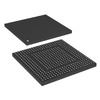
MPC8308CVMAFD
Freescale Semiconductor
MPU, 32-BIT, 266MHZ, PBGA473
SN75374N
Texas Instruments
IC GATE DRVR LOW-SIDE 16DIP
BQ20Z90DBTR
Texas Instruments
IC GAS GAUGE FOR BQ29330 30TSSOP
RP101K332D-TR
Nisshinbo Micro Devices Inc.
IC REG LIN 3.3V 300MA DFN1612-4B
HD64F3687HV
Renesas Electronics America Inc
IC MCU 16BIT 56KB FLASH 64QFP
2225SA332JAT1A\SB
KYOCERA AVX
CAP CER 3300PF 1.5KV NP0 2225
ST8034TDT
STMicroelectronics
IC INTERFACE SPECIALIZED 16SO
SRU1048-150Y
Bourns Inc.
FIXED IND 15UH 3.2A 29 MOHM SMD
MIC5213-3.6YC5-TR
Microchip Technology
IC REG LINEAR 3.6V 80MA SC70-5
MC34932EK
NXP USA Inc.
IC BRIDGE DRIVER PAR 54SOIC
TVP5146M2PFP
Texas Instruments
IC DIGITL VIDEO DECODER 80-HTQFP
BZX79C11
onsemi
DIODE ZENER 11V 500MW DO35