EP2S60F1020I4 Device Guide for Logic, Memory, and I/O
You get a clear look at what the EP2S60F1020I4 FPGA brings to your system and how it fits into demanding designs. This device packs a large amount of logic, memory, and I/O into one chip, letting you handle control, data movement, and processing at the same time. You can rely on steady timing, parallel operation, and flexible connections to build systems that stay responsive. From industrial platforms to communication hardware, this FPGA helps you combine performance and integration without adding extra components.Catalog
EP2S60F1020I4 Overview
The EP2S60F1020I4 is a high density programmable logic device designed to handle complex digital control and data processing tasks within a single chip. It offers a large pool of configurable logic, embedded memory, and flexible input and output connections packaged in a compact 1020 ball FBGA format. The device supports parallel operations and predictable hardware behavior, making it suitable for systems that require fast data handling and stable real time response. Common uses include industrial control platforms, communication equipment, and embedded systems where integration density and performance are balanced. Looking for EP2S60F1020I4? Contact us to check current stock, lead time, and pricing.
I/O Banks of EP2S60F1020I4
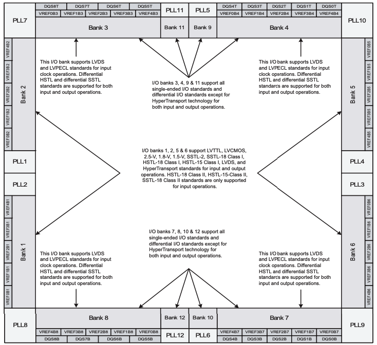
Divided into multiple numbered I O banks arranged around the device perimeter, the EP2S60F1020I4 groups input and output pins by shared voltage references and supported signaling standards. Banks 1, 2, 3, 4, 5, and 6 support LVDS and LVPECL for input clock operations, along with differential HSTL and SSTL standards for both input and output. Banks 3, 4, 7, 8, 9, 10, 11, and 12 additionally support single ended and differential standards, including LVTTL, LVCMOS, HSTL, SSTL, LVDS, and HyperTransport, with some standards limited to input operation. Dedicated PLL blocks are positioned adjacent to specific banks to enable clock generation and distribution, while VREF and DQS labeling indicates reference voltage and data strobe associations for memory and high speed interfaces.
EP2S60F1020I4 CAD Model
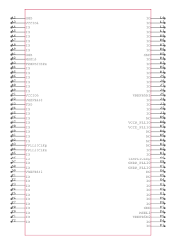
EP2S60F1020I4 Symbol
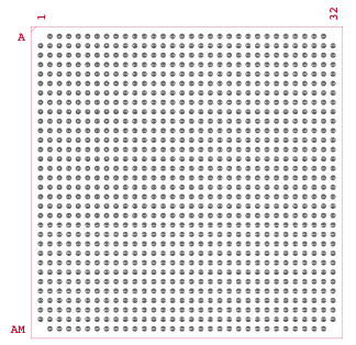
EP2S60F1020I4 Footprint
EP2S60F1020I4 3D Model

Features of EP2S60F1020I4
High Density Programmable Logic Architecture
The EP2S60F1020I4 is designed to support large digital systems within a single programmable device. Its structure allows many logic functions to be configured and executed at the same time, which helps reduce the need for additional supporting components. This approach supports compact system layouts while maintaining consistent behavior during operation.
Logic Capacity and Internal Organization
The device contains 60,440 logic elements organized into 3,022 logic array blocks. This internal arrangement supports orderly signal flow and stable timing behavior across complex designs. It allows designers to build structured control logic, data paths, and processing blocks without excessive internal congestion.
On Chip Memory Resources
A total of 2,544,192 bits of integrated memory is available for data storage and buffering tasks. This memory can be used for temporary data handling, lookup tables, or internal state storage. Having memory on the same device reduces reliance on external memory and shortens data access paths.
Extensive Input and Output Connectivity
Up to 718 user input and output pins are provided for connection to external devices and subsystems. This high pin count supports wide data interfaces and multiple control signals. It allows the device to interact with complex systems that require many external connections.
Core Voltage Operating Range
The core logic operates within a voltage range of 1.15 V to 1.25 V. This range supports stable internal operation while aligning with common low voltage digital system requirements. Proper voltage regulation helps maintain predictable behavior across operating conditions.
Surface Mount FBGA Package Format
The EP2S60F1020I4 is housed in a 1020 ball FBGA package with a 33 by 33 millimeter footprint. This package supports high connection density while keeping board space usage controlled. It is suited for multilayer boards where signal routing density is high.
Wide Operating Temperature Range
The device supports an operating junction temperature from minus 40 degrees Celsius to 100 degrees Celsius. This range allows reliable operation in environments with varying thermal conditions. It supports use in systems exposed to temperature changes over extended periods.
Deterministic Hardware Behavior
The internal structure is designed to deliver repeatable and predictable results during operation. Timing behavior remains consistent once configured, which supports systems that rely on fixed response patterns. This characteristic is useful in control oriented and real time digital designs.
Suitability for Demanding System Environments
The combination of logic capacity, memory resources, and wide connectivity supports use in complex embedded and industrial systems. The device is well suited for applications that require dense integration, stable operation, and long term reliability under continuous workloads.
EP2S60F1020I4 Technical Specifications
| Product Attribute | Attribute Value |
| Manufacturer | Intel |
| Voltage - Supply | 1.15V ~ 1.25V |
| Total RAM Bits | 2544192 |
| Supplier Device Package | 1020-FBGA (33x33) |
| Series | Stratix® II |
| Package / Case | 1020-BBGA |
| Package | Tray |
| Operating Temperature | -40°C ~ 100°C (TJ) |
| Number of Logic Elements/Cells | 60440 |
| Number of LABs/CLBs | 3022 |
| Number of I/O | 718 |
| Mounting Type | Surface Mount |
| Base Product Number | EP2S60 |
Block Diagram of EP2S60F1020I4
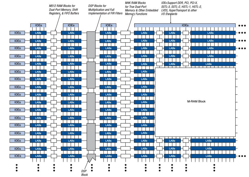
Arranged as a two dimensional programmable fabric, the EP2S60F1020I4 architecture is composed of repeating columns of Logic Array Blocks connected through a hierarchical routing network. Embedded within the logic fabric are M512 RAM blocks for small dual port memory, shift registers, and FIFO functions, along with larger M4K RAM blocks that support true dual port memory and general embedded storage. A centralized M RAM block provides higher density on chip memory for bulk data buffering. Dedicated DSP blocks are positioned near the center to support multiplication and filter operations without consuming general logic resources. Input and output elements are distributed around the device perimeter, enabling support for multiple signaling standards and high speed interfaces while maintaining balanced access to the internal logic and memory structure.
LAB Structure of EP2S60F1020I4
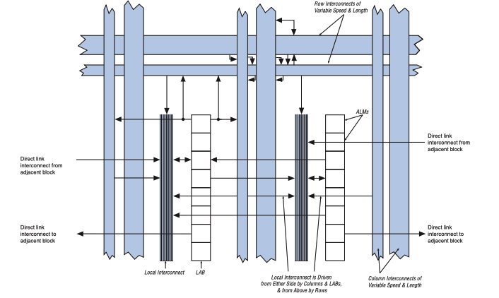
Organized around a Logic Array Block, the EP2S60F1020I4 structure groups multiple Adaptive Logic Modules connected through local, row, and column interconnects of varying lengths and speeds. Each LAB is linked to adjacent blocks through direct connections that reduce routing delay for neighboring logic. Local interconnect lines provide short, low latency paths within the LAB, while row and column interconnects enable signal distribution across larger regions of the device. Vertical connections allow signals to pass between LABs above and below, supporting flexible logic placement and predictable signal routing throughout the programmable fabric.
Applications of EP2S60F1020I4
Telecommunications Infrastructure Equipment
The EP2S60F1020I4 is used in fixed communication equipment that manages continuous data flow and structured signal handling. Its large logic capacity supports tasks such as packet processing, framing control, and timing coordination within base stations and network nodes. The wide input and output range allows direct connection to multiple data paths and control interfaces.
High Performance Embedded Computing Systems
In embedded computing platforms, this device combines control logic, data movement, and processing functions within a single programmable unit. It supports parallel operations that help manage complex workloads while keeping system behavior predictable. This makes it suitable for embedded systems that require dense integration and steady performance.
Industrial Automation and Control Systems
The EP2S60F1020I4 is applied in automation systems where coordinated control and fast response are required. It supports real time monitoring, sequencing, and control logic for machinery and process equipment. Its structure allows multiple control loops and data paths to operate together without interference.
Data Acquisition and Signal Processing Platforms
This device is well suited for platforms that collect and process large volumes of digital data. On chip memory supports buffering and intermediate storage, while parallel logic enables structured data handling. These characteristics help maintain consistent data flow in measurement and processing systems.
Networking and Switching Equipment
The high number of available input and output pins allows the EP2S60F1020I4 to interface with multiple ports and control signals. It supports fixed networking systems that require stable data routing and switching behavior. The device handles coordinated signal paths while maintaining predictable timing.
Aerospace and Defense Systems with Wide Temperature Operation
The supported temperature range allows use in systems exposed to changing thermal conditions. The device supports stable operation in environments where consistent behavior is required over long operating periods. This makes it suitable for hardware deployed in controlled and field based platforms.
Advantages and Disadvantages of EP2S60F1020I4
Advantages
• High logic density supports complex digital system integration
• Large number of user input and output pins simplifies wide system interfacing
• Substantial on chip memory reduces dependence on external memory devices
• Wide operating temperature range supports use in controlled and harsh environments
• Predictable timing behavior supports stable and repeatable system operation
Disadvantages
• Higher power consumption compared with lower density programmable devices
• Large FBGA package increases board layout complexity
• Requires careful power and thermal management in dense designs
• Not suited for applications that need compact or low pin count packages
EP2S60F1020I4 Alternatives
| Part Number | Manufacturer | Key Features | Use Case/Notes |
| EP2S60F1020I5 | Intel | High-density Stratix II FPGA with a large number of logic elements and embedded memory blocks. Designed for surface-mount assembly and reliable operation across industrial temperature ranges. | Used in telecom infrastructure, high-speed data processing, and advanced embedded systems that require strong compute performance. |
| EP2S60F1020C4 | Intel | Commercial-temperature Stratix II FPGA offering the same core architecture and memory resources as industrial versions, optimized for controlled environments. | Suitable for networking hardware, data acquisition systems, and compute platforms used in indoor or regulated conditions. |
| EP2S60F1020C4N | Intel | This variant retains the Stratix II high-performance logic architecture while supporting compact surface-mount packaging for dense PCB layouts. | Well suited for large embedded platforms, communication systems, and designs requiring high logic density with efficient board space usage. |
About Intel
Intel is a global technology company known for designing digital platforms used across computing, communications, and embedded systems. Its product portfolio covers programmable logic, processors, memory solutions, and supporting software that enable flexible system design and long service life. Intel focuses on scalable architectures that support a wide range of performance and integration needs, from embedded control to large data driven platforms. The company maintains extensive technical documentation and development ecosystems that support reliable design, validation, and long term system maintenance across many application domains.
Conclusion
The EP2S60F1020I4 stands out for its high logic density, wide I/O support, and strong on-chip memory resources. You can use it to handle complex control and data tasks while keeping timing behavior predictable. Its flexible I/O banks make it easier to connect different interfaces and signaling standards. The large FBGA package supports dense designs, though it does require careful planning. With support for wide temperature ranges, it fits systems that need stable operation over time. Overall, it gives you a solid balance of performance, integration, and reliability.
Datasheet PDF
EP2S60F1020I4 Datasheet:
About us
ALLELCO LIMITED
Read more
Quick inquiry
Please send an inquiry, we will respond immediately.
Frequently Asked Questions [FAQ]
1. What type of device is the EP2S60F1020I4?
It is a high-density FPGA designed for programmable digital logic, data handling, and control tasks.
2. How many logic elements does the EP2S60F1020I4 include?
The device contains 60,440 logic elements organized into multiple logic array blocks.
3. What makes the I/O structure flexible on this FPGA?
Its I/O banks support many single-ended and differential standards with shared voltage references.
4. Is the EP2S60F1020I4 suitable for real-time systems?
Yes, it offers predictable timing and parallel hardware behavior that work well in real-time designs.
5. Where is the EP2S60F1020I4 commonly used?
You often see it in industrial control systems, communication equipment, and high-performance embedded platforms.
EPM3256AQC208-10 Intel MAX 3000A Device Overview
on December 18th
Guide to the XC9572XL-10VQ64I CPLD
on December 18th
Popular Posts
-

Complex Instruction Set Computers: How They Changed Computing?
on April 18th 147765
-

USB-C Pinout and Features
on April 18th 111990
-

Using Xilinx Unified Simulation Primitives: A Comprehensive Guide to FPGA Design and Simulation
on April 18th 111351
-

Power Supply Voltages in Electronics: Meaning of VCC, VDD, VEE, VSS, and GND
on April 18th 83751
-

RJ45 Connector Guide: Pinout, Wiring, Cable Types, and Uses
on January 1th 79546
-

The Ultimate Guide to Wire Color Codes in Modern Electrical Systems
The way our electrical systems use colors isn’t just for looks. Each wire color now indicates a specific function, making it easier to identify and handle electrical components correctly during ins...on January 1th 66949
-

Purge Valve Guide: Function, Symptoms, Testing, and Replacement for Optimal Engine Performance
The purge valve is a key part of a car’s system that helps keep the air clean by managing fuel vapors before they can escape into the atmosphere. This not only helps the environment by reducing pol...on January 1th 63094
-

Quality (Q) Factor: Equations and Applications
The quality factor, or 'Q', is important when checking how well inductors and resonators work in electronic systems that use radio frequencies (RF). 'Q' measures how well a circuit minimizes energy...on January 1th 63028
-

Achieving Peak Performance with the Maximum Power Transfer Theorem
The Maximum Power Transfer Theorem explains how energy from a source, such as a battery or generator, flows to a connected load. It shows the exact condition where the load receives the most power....on January 1th 54092
-

A23 Battery Specifications and Compatibility
The A23 battery is a small, cylinder-shaped battery with high voltage. Also called 23A, 23AE, or MN21, it runs at 12 volts and much higher than AA or AAA batteries. Its special design make...on January 1th 52174
HOT Part Number
-

FSB50660SFT
Fairchild Semiconductor
AC MOTOR CONTROLLER, 8.1A
HMC1020LP4E
Analog Devices Inc.
IC RF DETECT 0HZ-3.9GHZ 24QFN
TPS75003RHLT
Texas Instruments
IC PWR MGMT TRIPLE-SUPPLY 20-QFN
2SC3646S-TD-E
onsemi
TRANS NPN 100V 1A PCP
SML013BDTT86
Rohm Semiconductor
LED BLUE CLEAR 3020 SMD
ISL9005IRFZ-T
Renesas Electronics America Inc
IC REG LINEAR 2.5V 300MA 8DFN
EP2AGX65DF25C6G
Intel
IC FPGA 252 I/O 572FBGA
VFC32KU/2K5
Texas Instruments
IC F/V & V/F CONV 100KHZ 14SOIC
AD7657BSTZ
Analog Devices Inc.
IC ADC 14BIT SAR 64LQFP
AD7899ARSZ-1REEL
Analog Devices Inc.
IC ADC 14BIT SAR 28SSOP
CL21C561JBANNND
Samsung Electro-Mechanics
CAP CER 560PF 50V NP0 0805
MIC5213-3.3BC5
Micrel Inc.
IC REG LINEAR MICROCAP LDO REG
MIC2505-2YM
Microchip Technology
IC PWR SWITCH N-CHAN 1:1 8SOIC
P2020NSN2KFC
NXP USA Inc.
IC MPU QORIQ P2 1.2GHZ PBGA689
SN74ALS156N
Texas Instruments
IC DECODER/DEMUX 2X1:4 16DIP
NCP103AMX185TCG
onsemi
IC REG LINEAR 1.85V 150MA 4UDFN
MCR10EZPJ474
Rohm Semiconductor
RES SMD 470K OHM 5% 1/8W 0805
DG200BDJ-E3
Vishay Siliconix
IC SWITCH SPST-NCX2 85OHM 14DIP -

IRLHS2242TR2PBF
Infineon Technologies
MOSFET P-CH 20V 5.8A 2X2 PQFN
ICL3245ECA-T
Intersil
IC TRANSCEIVER FULL 3/5 28SSOP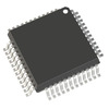
AD1886AJSTZ
Analog Devices Inc.
IC CODEC STEREO 16BIT 48LQFP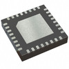
MAX3955ETJ+T
Analog Devices Inc./Maxim Integrated
IC TRANSCEIVER 2/2 32TQFN
MAX9637AXA+T
Analog Devices Inc./Maxim Integrated
IC CMOS 2 CIRCUIT SC70-8
19C500PG1L
Honeywell Sensing and Productivity Solutions
SENSOR 500PSIG 0.1V
BR93L86RFJ-WE2
Rohm Semiconductor
IC EEPROM 16KBIT SPI 2MHZ 8SOPJ
964261-2
H&L Manufacturing
964261-2 TE TERMINAL
TC427EOA
Microchip Technology
IC GATE DRVR LOW-SIDE 8SOIC
04025A151MAT2A
KYOCERA AVX
CAP CER 150PF 50V NP0 0402
S34ML02G100TFI000
Cypress Semiconductor Corp
IC FLASH 2GBIT PARALLEL 48TSOP
TL7759CDR
Texas Instruments
IC SUPERVISOR 1 CHANNEL 8SOIC
MCIMX353DVM5B
Freescale Semiconductor
I.MX35 32-BIT MPU, ARM1136JF-S C
ICL7665SIBAZ-T
Renesas Electronics America Inc
IC SUPERVISOR 2 CHANNEL 8SOIC
AD7533JN
Harris Corporation
AD7533 - MULTIPLYING D/A CONVERT
SI4432-B1-FMR
Silicon Labs
IC RF TXRX ISM<1GHZ 20VFQFN
MAX3460ESD+
Analog Devices Inc./Maxim Integrated
IC TRANSCEIVER FULL 1/1 14SOIC
AS7C34096A-10JCN
Alliance Memory, Inc.
IC SRAM 4MBIT PARALLEL 36SOJ -

NCP3418ADR2G
onsemi
IC GATE DRVR HALF-BRIDGE 8SOIC
DMN5L06WK-7
Diodes Incorporated
MOSFET N-CH 50V 300MA SOT323
CL10C151JB8NCNC
Samsung Electro-Mechanics
CAP CER 150PF 50V C0G/NP0 0603
12105C225MAZ2A
KYOCERA AVX
CAP CER 2.2UF 50V X7R 1210
PSB21150FV1.4
Lantiq
PSB21150 - IPAC-X ISDN PC ADAPTE
SN74SSTV16857DGGR
Texas Instruments
IC REG BUFFER 14-BIT 48-TSSOP
AD5433YRUZ-REEL
Analog Devices Inc.
IC DAC 10BIT A-OUT 20TSSOP
MAX261BCNG+
Analog Devices Inc./Maxim Integrated
IC FILTER 57KHZ UNIV SWTCH 24DIP
LM3S1162-IQC50-A2T
Texas Instruments
IC MCU 32BIT 64KB FLASH 100LQFP
AP432SAG-7
Diodes Incorporated
IC VREF SHUNT ADJ SOT23-3
XC7Z020-L1CLG484I
AMD
IC SOC CORTEX-A9 667MHZ 484BGA
VI-26Z-CU
Vicor Corporation
DC DC CONVERTER 2V 40W
ADG212AKR-REEL
Analog Devices Inc.
IC SW SPST-NOX4 115OHM 16SOIC
DNF18-206FIB-3K
Panduit Corp
CONN QC RCPT 18-22AWG 0.187
NTMD4184PFR2G
onsemi
DUAL P-CHANNEL FETKY POWER MOSFE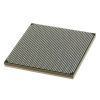
XC7V2000T-L2FLG1925E
Xilinx Inc.
IC FPGA 1200 I/O 1925FCBGA
TPS53661RSBT
Texas Instruments
IC REG CTRLR VR12 1OUT 40WQFN
TPA711DGN
Texas Instruments
IC AMP CLASS AB MONO 700MW 8MSOP