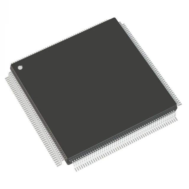
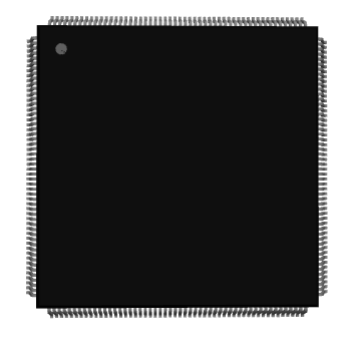
EPM3256AQC208-10 Intel MAX 3000A Device Overview
You get a programmable logic device that helps you combine many fixed logic functions into one flexible chip. The EPM3256AQC208-10 lets you manage control paths, timing signals, and interfaces without redesigning hardware each time logic needs to change. You can update the logic after installation, which makes adjustments easier during testing or later use. With a clear structure, steady timing, and a high pin count, this device fits well in systems that need reliable digital control without the complexity of larger programmable platforms.Catalog
EPM3256AQC208-10 Overview
The EPM3256AQC208-10 is a programmable logic device designed to handle mid-level digital control and interface tasks within a single component. It combines configurable logic resources with predictable timing behavior, allowing multiple fixed logic functions to be consolidated into one flexible design. The device supports updates after installation, which helps accommodate design changes without hardware replacement. It is commonly applied in control circuits, interface adaptation, address decoding, and simple sequencing functions. Its structure favors stable signal handling and consistent response, making it suitable for systems that rely on defined logic paths rather than high-density processing. Looking for EPM3256AQC208-10? Contact us to check current stock, lead time, and pricing.
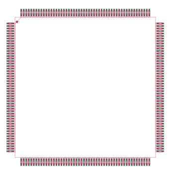
Pin-Out Diagram of EPM3256AQC208-10
[IMAGE OF 208–Pin PQFP Package Pin-Out Diagram]
Square package layout defines the physical pin arrangement for the 208 pin plastic quad flat pack used by the device, with pins distributed evenly along all four sides. Pin 1 is marked at the upper left corner, and numbering proceeds sequentially around the package perimeter, with reference points shown at pins 53, 105, and 157 to indicate side transitions. The package outline is identified as not drawn to scale, emphasizing orientation and numbering rather than dimensions. Central labeling identifies compatible device variants, while the symmetrical lead structure supports high pin count connectivity for power, ground, and user I O signals.
EPM3256AQC208-10 CAD Model
EPM3256AQC208-10 Symbol
EPM3256AQC208-10 Footprint
EPM3256AQC208-10 3D Model
Features of EPM3256AQC208-10
MAX 3000A CPLD Family Membership
The device is part of the MAX 3000A CPLD family, which is designed for stable digital logic control and interface tasks. This family focuses on predictable behavior and repeatable timing, making it suitable for systems that require consistent logic operation. It allows multiple fixed logic functions to be combined into one configurable device, reducing circuit complexity.
In-System Programmable Architecture
The EPM3256AQC208-10 supports in-system programming, allowing logic configurations to be written, updated, or corrected after the device is installed on a circuit board. This capability supports design changes without hardware replacement and simplifies updates during development or maintenance. It also helps reduce downtime when logic adjustments are needed.
Fast Propagation Delay Performance
The device offers a maximum propagation delay of 10 ns, enabling rapid response between logic inputs and outputs. This supports applications that depend on timely signal transitions and controlled response paths. The consistent delay behavior helps maintain reliable operation in synchronous and control-based designs.
Internal Operating Voltage Range
The internal logic operates within a voltage range of 3.0 V to 3.6 V, aligning with common low-voltage digital systems. This range supports stable logic operation while maintaining compatibility with surrounding components. It also helps manage power behavior in compact digital designs.
Macrocell-Based Logic Resources
A total of 256 macrocells are available to implement programmable logic functions. These macrocells support combinational and registered logic, allowing flexible implementation of control logic and interface functions. This capacity suits mid-level logic requirements without the overhead of larger programmable devices.
Organized Logic Block Structure
The internal architecture is arranged into 16 logic blocks, providing a structured approach to logic placement and signal flow. This organization helps maintain predictable timing and simplifies the management of logic paths. It supports orderly design implementation for control and sequencing tasks.
Usable Logic Gate Capacity
The device provides approximately 5000 usable logic gates, enabling it to replace several discrete logic components within a single package. This consolidation helps reduce board space and simplifies system layout. It is well suited for designs that require moderate logic complexity.
High User Input Output Availability
The EPM3256AQC208-10 includes 158 user input and output pins, allowing extensive connection to external signals and devices. This high pin count supports complex interfacing needs such as address decoding, bus control, and signal routing. It enables flexible integration within larger digital systems.
Surface Mount PQFP Package
The device is housed in a 208 pin PQFP surface mount package designed for dense circuit board layouts. This package supports reliable electrical connections while fitting into s
EPM3256AQC208-10 Technical Specifications
| Product Attribute | Attribute Value |
| Manufacturer | Intel |
| Voltage Supply - Internal | 3V ~ 3.6V |
| Supplier Device Package | 208-PQFP (28x28) |
| Series | MAX® 3000A |
| Programmable Type | In System Programmable |
| Package / Case | 208-BFQFP |
| Package | Tray |
| Operating Temperature | 0°C ~ 70°C (TA) |
| Number of Macrocells | 256 |
| Number of Logic Elements/Blocks | 16 |
| Number of I/O | 158 |
| Number of Gates | 5000 |
| Mounting Type | Surface Mount |
| Delay Time tpd(1) Max | 10 ns |
| Base Product Number | EPM3256 |
Device Block Diagram of EPM3256AQC208-10
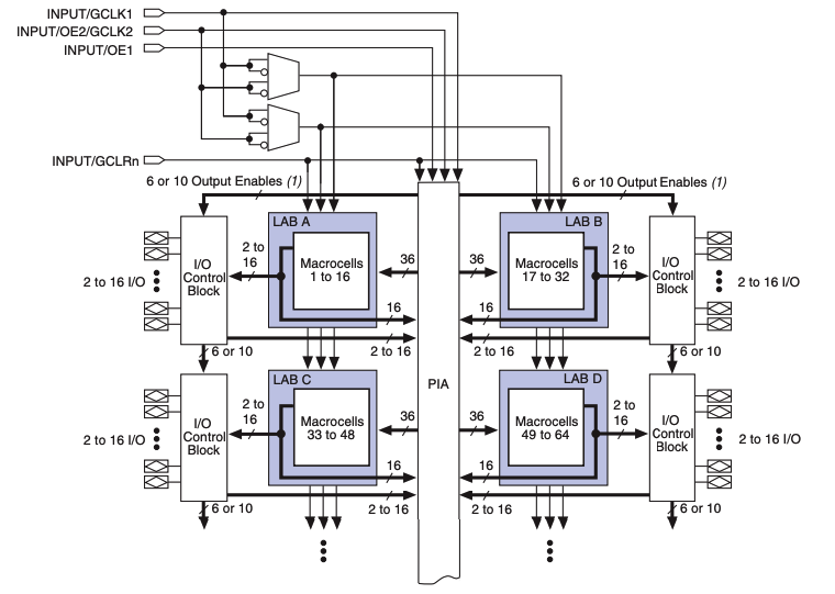
Internal architecture is organized around multiple Logic Array Blocks labeled A through D, each containing groups of macrocells used to implement programmable logic functions. Macrocells are connected through a central Programmable Interconnect Array that provides routing paths between logic blocks and distributes signals across the device. I/O Control Blocks are positioned around the logic array and manage data flow between internal logic and external pins, supporting configurable input, output, and bidirectional operation. Global control lines at the top handle clock distribution, output enable control, and global clear functions, allowing synchronized operation across all logic blocks. Signal width annotations indicate the number of available routing and enable lines between blocks, reflecting the fixed, predictable structure used throughout the MAX 3000A family.
Macrocell of EPM3256AQC208-10
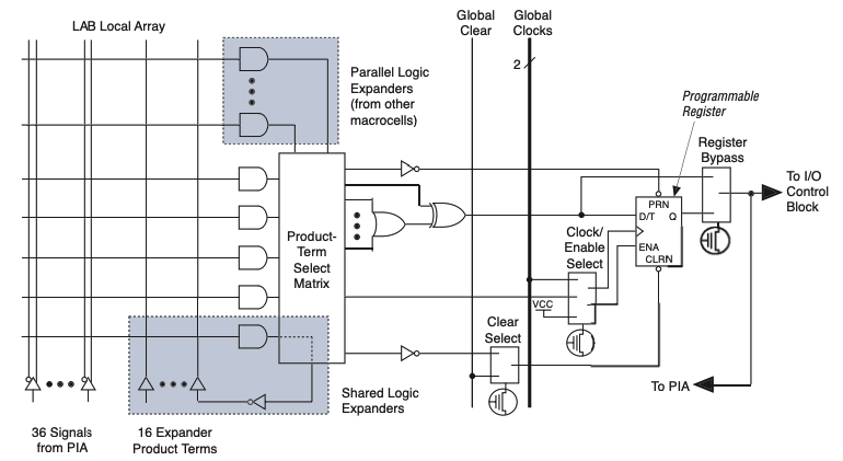
Macrocell structure combines a product term select matrix with parallel and shared logic expanders to form configurable combinational logic within a Logic Array Block. Input signals arrive from the Programmable Interconnect Array and local LAB routing, feeding up to sixteen product terms that are combined through selectable logic paths. The output can be routed either directly or through a programmable register that includes clock enable, clear control, and access to global clock and global clear signals. A register bypass path allows purely combinational operation, while controlled feedback routes the result back to the interconnect array or toward the I/O control block for external connection.
AC Test Conditions of EPM3256AQC208-10
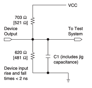
Test configuration defines the external circuit used to measure AC performance of device input and output paths under controlled conditions. A resistive network connects the device output to the supply and ground using specified resistor values that differ for 2.5 V and 3.3 V operation, establishing known load characteristics. A capacitor connected to ground represents total load capacitance, including test fixture effects, while the measurement node interfaces with the test system. The setup constrains input rise and fall times to less than two nanoseconds and minimizes noise caused by ground current transients during output switching, ensuring consistent and repeatable AC timing results.
Applications of EPM3256AQC208-10
Glue Logic Replacement for Discrete Components
The EPM3256AQC208-10 is commonly used to replace collections of fixed logic devices such as gates, decoders, and multiplexers. By consolidating these functions into one programmable device, system layouts become simpler and easier to manage. Logic behavior can also be adjusted through reprogramming, which supports design refinement without hardware changes.
Address Decoding and Control in Embedded Systems
In embedded systems, the device handles address decoding and control tasks that coordinate memory, peripherals, and control signals. It helps direct data flow and manage enable signals with consistent timing. This makes it suitable for systems that rely on clear separation of address spaces and predictable control behavior.
Bus Interfacing and Protocol Adaptation
The device is applied in bus interfacing roles where different signal formats or timing requirements must work together. It supports signal conditioning, routing, and basic protocol translation between subsystems. This helps maintain orderly communication paths within mixed or legacy digital environments.
Industrial Control Panels and Automation Equipment
Within industrial control panels, the EPM3256AQC208-10 manages sequencing, interlock logic, and status monitoring. Its stable timing supports coordinated operation of sensors, actuators, and control signals. The device fits well in automation equipment that values reliable logic operation over high processing complexity.
Telecommunications Support Logic Functions
The device serves as support logic in telecommunications systems, handling timing control, interface coordination, and auxiliary digital functions. It helps organize signal relationships between functional blocks. This role supports consistent operation in communication equipment that depends on orderly digital control.
Consumer Electronics Control and Timing
In consumer electronics, the device is used for control and timing functions such as input handling, mode selection, and system coordination. Its programmable nature allows one design to support multiple product variations. This flexibility supports compact and adaptable consumer devices.
Legacy System Maintenance and Redesign
The EPM3256AQC208-10 is well suited for maintaining or updating legacy systems that require pin-compatible programmable logic. It allows existing hardware layouts to remain unchanged while logic behavior is revised. This approach helps extend system life while keeping redesign effort manageable.
EPM3256AQC208-10 Advantages and Disadvantages
Advantages
• In-system programmability supports logic updates without removing the device
• Maximum 10 ns delay enables responsive digital signal handling
• High number of I O pins supports broad external connectivity
• Predictable timing behavior supports stable control logic operation
• Suitable for glue logic, control functions, and interface bridging
• PQFP package supports easier inspection and assembly compared to array packages
Disadvantages
• Limited logic resources compared to newer programmable logic devices
• Operation restricted to a commercial temperature range from 0 C to 70 C
• Higher power usage than more recent low-power logic solutions
• Larger package footprint compared to modern compact alternatives
• Fewer integration features than advanced programmable platforms
EPM3256AQC208-10 Alternatives
| Part Number | Manufacturer | Key Features | Use Case/Notes |
| EPM3256AQI208-10 | Intel | Member of the MAX 3000A CPLD family with 256 macrocells, in-system programmability, and stable 3 V operation for reliable logic control. | Used in industrial and embedded systems for glue logic, interface control, and moderate-speed digital designs. |
| EPM3256AQI208-10N | Intel | Same logic density and architecture as other EPM3256 devices, with predictable timing and flexible I/O handling. | Suitable for legacy designs and embedded platforms that require dependable CPLD-based logic integration. |
| EPM3256AQC208-7N | Intel | Faster speed-grade variant offering lower propagation delay while maintaining the same macrocell and I/O structure. | Ideal for timing-sensitive logic such as bus arbitration, state machines, and performance-critical control paths. |
About Intel
Intel is a global technology company known for developing a wide range of digital computing and programmable logic products. Its portfolio spans processors, programmable devices, and system solutions used across computing, communications, and industrial markets. The company has a long history of advancing digital design tools and platforms that support reliable system development. Through continuous investment in process technology and product integration, Intel supports scalable solutions that serve both embedded systems and high-performance applications. Its product families are widely adopted in systems that value consistency, long-term support, and broad ecosystem compatibility.
Conclusion
The EPM3256AQC208-10 offers a clear way to handle mid-level digital logic in one device. You can replace groups of fixed logic parts while keeping timing behavior steady and easy to predict. Its macrocell-based design gives you enough room for control, decoding, and interface tasks. The 208-pin package also supports wide signal access when connections matter. With in-system programming, you can adjust logic without touching the board. Overall, it gives you a practical balance of flexibility and structure for long-term use.
Datasheet PDF
EPM3256AQC208-10 Datasheet:
About us
ALLELCO LIMITED
Read more
Quick inquiry
Please send an inquiry, we will respond immediately.
Frequently Asked Questions [FAQ]
1. What type of device is the EPM3256AQC208-10?
It is a CPLD that combines programmable logic functions into a single chip for control and interface tasks.
2. Can the EPM3256AQC208-10 be reprogrammed after installation?
Yes, it supports in-system programming, so you can update the logic while it is already on the board.
3. How many macrocells does the EPM3256AQC208-10 have?
The device includes 256 macrocells for building combinational and registered logic.
4. What package is used for the EPM3256AQC208-10?
It comes in a 208-pin PQFP surface-mount package.
5. Where is the EPM3256AQC208-10 commonly used?
It is often used for glue logic, address decoding, bus control, and general digital control functions.
Understanding Film Capacitors for Everyday Circuits
on December 18th
EP2S60F1020I4 Device Guide for Logic, Memory, and I/O
on December 18th
Popular Posts
-

Complex Instruction Set Computers: How They Changed Computing?
on April 17th 147710
-

USB-C Pinout and Features
on April 17th 111653
-

Using Xilinx Unified Simulation Primitives: A Comprehensive Guide to FPGA Design and Simulation
on April 17th 111314
-

Power Supply Voltages in Electronics: Meaning of VCC, VDD, VEE, VSS, and GND
on April 17th 83575
-

RJ45 Connector Guide: Pinout, Wiring, Cable Types, and Uses
on January 1th 79214
-

The Ultimate Guide to Wire Color Codes in Modern Electrical Systems
The way our electrical systems use colors isn’t just for looks. Each wire color now indicates a specific function, making it easier to identify and handle electrical components correctly during ins...on January 1th 66745
-

Quality (Q) Factor: Equations and Applications
The quality factor, or 'Q', is important when checking how well inductors and resonators work in electronic systems that use radio frequencies (RF). 'Q' measures how well a circuit minimizes energy...on January 1th 62923
-

Purge Valve Guide: Function, Symptoms, Testing, and Replacement for Optimal Engine Performance
The purge valve is a key part of a car’s system that helps keep the air clean by managing fuel vapors before they can escape into the atmosphere. This not only helps the environment by reducing pol...on January 1th 62792
-

Achieving Peak Performance with the Maximum Power Transfer Theorem
The Maximum Power Transfer Theorem explains how energy from a source, such as a battery or generator, flows to a connected load. It shows the exact condition where the load receives the most power....on January 1th 54020
-

A23 Battery Specifications and Compatibility
The A23 battery is a small, cylinder-shaped battery with high voltage. Also called 23A, 23AE, or MN21, it runs at 12 volts and much higher than AA or AAA batteries. Its special design make...on January 1th 51936
HOT Part Number
-

FTSH-140-01-L-DV
Samtec Inc.
CONN HEADER SMD 80POS 1.27MM
XCS05XL-4VQ100I
AMD
IC FPGA 77 I/O 100VQFP
MMA02040C1243FB300
Vishay Beyschlag/Draloric/BC Components
RES 124K OHM 1% 2/5W MELF 0204
LQP03HQ1N1W02D
Murata Electronics
FIXED IND 1.1NH 1.1A 40MOHM SMD
FSFR2100USL
Fairchild Semiconductor
IC OFFLINE SW HALF-BRIDGE 9SIP
M29W256GH7AN6E
Micron Technology Inc.
IC FLASH 256MBIT PARALLEL 56TSOP
VI-JWY-EX
Vicor Corporation
DC DC CONVERTER 3.3V 50W
1N4740A-T
Diodes Incorporated
DIODE ZENER 10V 1W DO41
CC0402JRNPO7BN391
Yageo
CAP CER 390PF 16V NPO 0402
MAX4522CSE+T
Analog Devices Inc./Maxim Integrated
IC SW SPST-NOX4 100OHM 16SOIC
ADR03BRZ-REEL7
Analog Devices Inc.
IC VREF SERIES 0.1% 8SOIC
FQB55N10TM
Fairchild Semiconductor
POWER FIELD-EFFECT TRANSISTOR, 5
93C56BT-I/SN
Microchip Technology
IC EEPROM 2KBIT MICROWIRE 8SOIC
TOP253GN
Power Integrations
IC OFFLINE SWITCH FLYBACK 8SMD
12107A680JAT2A
AVX Corporation
CAP CER 68PF 500V NP0 1210
LM2574HVM-5.0
Texas Instruments
IC REG BUCK 5V 500MA 14SOIC
EMK042CG150JC-F
Taiyo Yuden
CAP CER 15PF 16V C0G/NP0 01005
SPC560P40L3BEAAY
STMicroelectronics
IC MCU 32BIT 256KB FLASH 100LQFP -
C4532X7R2E334K230KA
TDK Corporation
CAP CER 0.33UF 250V X7R 1812
W25Q16DVZPIG
Winbond Electronics
IC FLASH 16MBIT SPI/QUAD 8WSON
IXFH6N100F
IXYS
MOSFET N-CH 1000V 6A TO247
GRM0335C1H7R5DD01D
Murata Electronics
CAP CER 7.5PF 50V C0G/NP0 0201
ULQ2003ADG4
Texas Instruments
IC PWR DRIVER NPN 1:1 16SOIC
SZMM3Z3V6T1G
onsemi
DIODE ZENER 3.6V 300MW SOD323
DCF010-TL-E
onsemi
DIODE ARRAY GP 80V 100MA 3MCP
EPF10K50RC240-4N
Intel
IC FPGA 189 I/O 240RQFP
MAX8686ETL+T
Analog Devices Inc./Maxim Integrated
IC REG BUCK ADJ 25A 40TQFN
LTC2209IUP
Analog Devices Inc.
IC ADC 16BIT PIPELINED 64QFN
ADM696ARZ-REEL
Analog Devices Inc.
IC SUPERVISOR 1 CHANNEL 16SOIC
MUR130RLG
onsemi
DIODE GEN PURP 300V 1A AXIAL
1808N220J302LT
Walsin Technology Corporation
CAP CER 22PF 3KV C0G/NP0 1808
TC54VC2502ECB713
Microchip Technology
IC SUPERVISOR 1 CHANNEL SOT23A-3
SCP6SMB68AT3G
Littelfuse Inc.
TVS DIODE SMB
NPH15S4812IC
Murata Power Solutions Inc.
DC DC CONVERTER 12.1V 15W
1SMB5935BT3
onsemi
DIODE ZENER 27V 3W SMB
C3216X7R1E475K085AB
TDK Corporation
CAP CER 4.7UF 25V X7R 1206 -
74437346015
Würth Elektronik
FIXED IND 1.5UH 7.2A 15 MOHM SMD
FOD3150SD
onsemi
OPTOISO 5KV 1CH GATE DRIVER 8SMD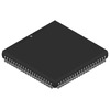
TN80C186EB-16
Rochester Electronics, LLC
MICROPROCESSOR, 16-BIT, 16MHZ, C
SN7407D
Texas Instruments
IC BUF NON-INVERT 5.25V 14SOIC
TLRZ1JTTD
KOA Speer Electronics, Inc.
RES 0 OHM JUMPER 0603
RT1206DRE074K99L
YAGEO
RES SMD 4.99K OHM 0.5% 1/4W 1206
06031A221JAT4A
KYOCERA AVX
CAP CER 220PF 100V C0G/NP0 0603
MC33886VWR2
Freescale Semiconductor
STEPPER MOTOR CONTROLLER
PTZTE2536B
Rohm Semiconductor
DIODE ZENER 39.2V 1W PMDS
PS2806-4-A
CEL
OPTOISOLTR 2.5KV 4CH DARL 16SOIC
GCM1885C1H5R8DA16D
Murata Electronics
CAP CER 5.8PF 50V C0G/NP0 0603
SY88813VKG
Microchip Technology
IC LIMIT AMP 10MSOP
MAX4603EAE+T
Analog Devices Inc./Maxim Integrated
IC SW SPST-NO/NCX4 2.5OHM 16SSOP
ADF4002BCPZ-RL
Analog Devices Inc.
IC CLK/FREQ SYNTH 20LFCSP
SNJ54HC164J
Texas Instruments
54HC164 8-BIT PARALLEL-OUT SERIA
TVB035RSC-L
Littelfuse Inc.
THYRISTOR 35V 400A DO214AA
NCV1117ST18T3G
onsemi
IC REG LINEAR 1.8V 1A SOT223
293D107X0010D2TE3
Vishay Sprague
CAP TANT 100UF 20% 10V 2917