EP2S60F672C4 FPGA: Features, Applications, Programming & Datasheet Guide
In this guide, you’ll get a clear overview of the EP2S60F672C4, a powerful FPGA from Intel’s Stratix II family. You’ll learn about its main features, architecture, block structure, and technical specs to understand how it fits into advanced digital designs. It also walks you through its programming steps, applications, advantages, and disadvantages so you can see exactly where and how this device can be used.Catalog
What is the EP2S60F672C4?
The EP2S60F672C4 is a high-density FPGA from Intel (formerly Altera), belonging to the Stratix II family. Built on a 90 nm, 1.2 V copper SRAM process, it delivers substantial logic capacity within a 672-ball FBGA package, making it ideal for complex digital systems. As part of the EP2S series, the “60” device sits in the mid-to-upper range of the Stratix II lineup, offering a strong balance of logic density, embedded memory, and I/O resources. Known for its robust architecture and reliability, this FPGA remains a trusted choice in many advanced designs.
Looking for EP2S60F672C4? Contact us to check current stock, lead time, and pricing.
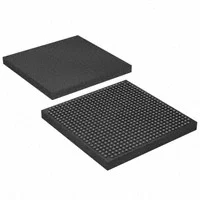
EP2S60F672C4 CAD Models
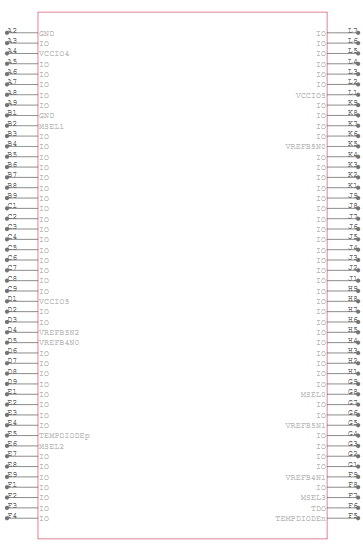
EP2S60F672C4 Symbol
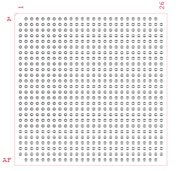
EP2S60F672C4 Footprint
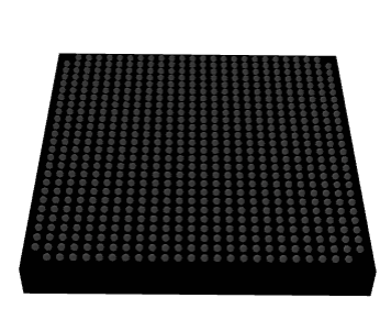
EP2S60F672C4 3D Model
EP2S60F672C4 Features
• Advanced 90 nm, 1.2 V CMOS Process
EP2S60F672C4 is fabricated on a 90 nm all-layer copper CMOS process that runs at a 1.2 V core voltage. This technology enables high speed, reduced power consumption, and greater logic density compared to older FPGA generations.
• Adaptive Logic Module (ALM) Architecture
The device uses ALMs as its logic building block instead of traditional logic elements. This architecture improves resource utilization, allowing more complex logic functions to be implemented efficiently within the same silicon area.
• High Logic Density
With approximately 60,440 logic elements (24,176 ALMs), the FPGA supports large and sophisticated digital designs. This high capacity makes it suitable for applications such as signal processing, communications, and embedded control systems.
• TriMatrix™ On-Chip Memory
EP2S60F672C4 integrates three types of RAM blocks, (M512, M4K, and M-RAM) to provide a total of around 2.4 Mbits of embedded memory. This mix allows to implement small FIFOs, medium buffers, and large dual-port memories efficiently.
• Dedicated DSP Blocks
The device includes 36 dedicated DSP blocks designed for arithmetic operations like multiplications, accumulations, and FIR filtering. These blocks boost performance in computation-intensive tasks while saving general logic resources.
• High-Speed I/O and Signal Integrity
It supports various single-ended and differential I/O standards along with dynamic phase alignment (DPA) circuitry. These features enable stable, high-speed data transfer up to 1 Gbps, ensuring reliable communication with external components.
• Rich External Memory Interface Support
The FPGA is compatible with DDR, DDR2, QDR II, RLDRAM II, and other memory standards. Built-in interface support simplifies board design and achieves high data throughput for memory-intensive applications.
• Flexible Clock Management
Up to 12 on-chip PLLs allow clock multiplication, division, phase shifting, and glitch-free switchover. You can fine-tune clock domains and reduce jitter, supporting internal clock frequencies of up to 500–550 MHz.
• Bitstream Encryption and Reconfiguration
EP2S60F672C4 supports AES-based bitstream encryption to secure intellectual property. It also offers remote reconfiguration capability, enabling in-field updates without replacing the device.
Stratix II Block Diagram
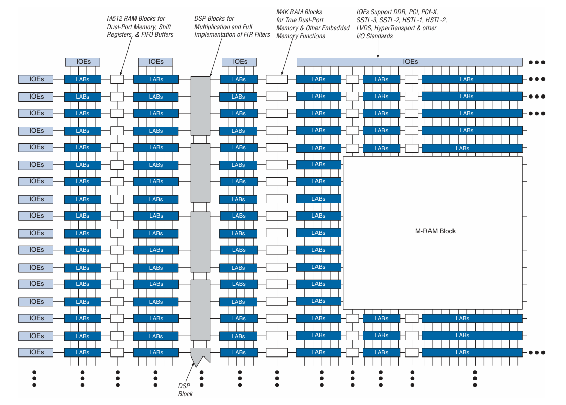
The Stratix II block diagram, as shown for EP2S60F672C4, illustrates the internal arrangement of logic, memory, and DSP resources that form the FPGA’s core. Logic Array Blocks (LABs) are arranged in a regular grid, surrounded by embedded RAM and DSP columns, which provide fast arithmetic and on-chip storage capabilities. Peripheral I/O elements and clock networks frame this structure, enabling efficient data transfer and timing control between the FPGA and external devices.
Stratix II I/O Banks Diagram
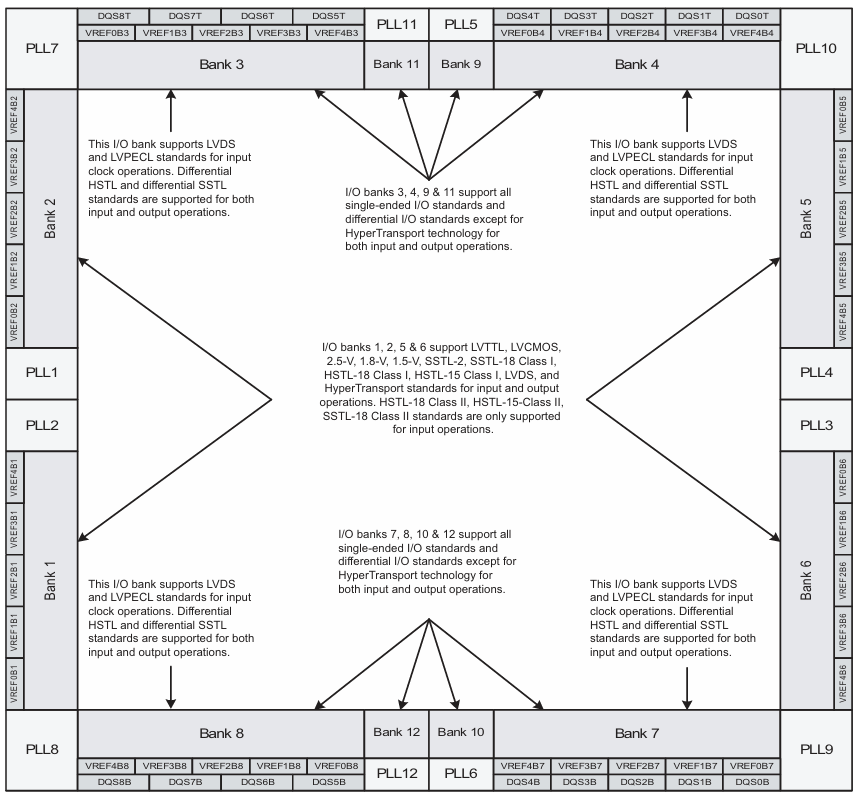
This Stratix II I/O Banks Diagram illustrates how the input/output pins of the EP2S60F672C4 are grouped and what electrical standards each group supports. Each I/O bank is designed to handle specific voltage levels, signaling types, and functions such as LVTTL, SSTL, LVDS, or clock input standards. The layout shows how different banks (e.g., 1, 2, 5, 6 vs. 3, 4, 7, 8, etc.) are optimized for either general-purpose I/O or high-speed differential signaling, including support for LVDS/LVPECL clock inputs at the edges.
EP2S60F672C4 Specifications
|
Type |
Parameter |
|
Manufacturer |
Altera/Intel |
|
Series |
Stratix® II |
|
Packaging |
Tray |
|
Part Status |
Obsolete |
|
Number of LABs/CLBs |
3022 |
|
Number of Logic Elements/Cells |
60,440 |
|
Total RAM Bits |
2,544,192 |
|
Number of I/O |
492 |
|
Voltage – Supply |
1.15 V ~ 1.25 V |
|
Mounting Type |
Surface Mount |
|
Operating Temperature |
0 °C ~ 85 °C (TJ) |
|
Package / Case |
672-BBGA |
|
Supplier Device Package |
672-FBGA (27 × 27) |
|
Base Product Number |
EP2S60 |
EP2S60F672C4 Applications
1. Digital Signal Processing (DSP) and Filtering
EP2S60F672C4 is well suited for implementing high-performance DSP functions such as FIR and IIR filters, FFT processing, and complex arithmetic operations. Its dedicated DSP blocks handle multiplications and accumulations efficiently, freeing general logic resources for other tasks. The on-chip TriMatrix™ memory enables smooth data buffering and pipelining, which is great for real-time processing at high sample rates. This makes the device ideal for advanced audio, video, and radar signal applications.
2. High-Speed Communication and Networking
The FPGA’s high-speed I/O interfaces and dynamic phase alignment (DPA) circuitry support reliable, gigabit-level data transmission. It can implement communication protocols and physical layer functions for systems like routers, switches, and backplane interconnects. With its large logic capacity and flexible PLLs, it can manage complex timing and protocol conversions between multiple high-speed interfaces. These capabilities make it a strong fit for telecom infrastructure and high-bandwidth networking equipment.
3. Memory Controllers and Data Processing Systems
EP2S60F672C4 supports various external memory interfaces including DDR, DDR2, RLDRAM II, and QDR II, making it ideal for designing high-bandwidth memory controllers. It can handle data buffering, address generation, and arbitration at high speeds with minimal latency. The combination of fast clock networks and embedded RAM blocks allows efficient management of large data streams. This makes the FPGA suitable for image processing, video streaming, and scientific computation platforms that rely on heavy data throughput.
4. Custom Logic and Embedded Acceleration
With over 60,000 logic elements and rich clock management, the FPGA can host customized hardware accelerators for specific algorithms. Designers often use it to offload computationally intensive tasks from CPUs, such as encryption, protocol parsing, or real-time control loops. It can also integrate multiple functional blocks, making it suitable for complex SoC-like designs. This flexibility makes it valuable in applications like industrial automation, security systems, and aerospace control units.
5. Prototyping and Educational Development Platforms
The EP2S60 device is commonly found on FPGA development kits used for prototyping, testing, and academic research. Its balance of logic capacity, I/O count, and DSP capabilities allows engineers and students to implement and verify full systems on a single chip. It supports rapid iteration of digital designs, enabling hardware verification before committing to ASIC development. Many universities and R&D labs use it to teach advanced digital design and signal processing concepts.
EP2S60F672C4 Similar Parts
|
Specification |
EP2S60F672C4 |
EP2S60F672C3N |
EP2S60F672C5 |
EP2S60F672C5N |
EP2S60F672I4
|
EP2S60F672I3N |
|
Family / Series |
Stratix II |
Stratix II |
Stratix II |
Stratix II |
Stratix II |
Stratix II |
|
Logic Elements (LE) |
60,440 |
60,440 |
60,440 |
60,440 |
60,440 |
60,440 |
|
ALMs |
24,176 |
24,176 |
24,176 |
24,176 |
24,176 |
24,176 |
|
Package |
FBGA-672 |
FBGA-672 |
FBGA-672 |
FBGA-672 |
FBGA-672 |
FBGA-672 |
|
Speed Grade |
C4 (Std) |
C3 (Faster) |
C5 (Faster) |
C5 (Faster) |
I4 (Std) |
I3 (Faster) |
|
Temperature Grade |
Commercial (0 ~ 70 °C) |
Commercial |
Commercial |
Commercial |
Industrial (−40 ~ 100 °C) |
Industrial (−40 ~ 100 °C) |
|
I/O Pins |
492 |
492 |
492 |
492 |
492 |
492 |
|
On-Chip Memory |
2.4 Mbit |
2.4 Mbit |
2.4 Mbit |
2.4 Mbit |
2.4 Mbit |
2.4 Mbit |
|
Core Voltage |
1.2 V |
1.2 V |
1.2 V |
1.2 V |
1.2 V |
1.2 V |
|
Key Difference |
Baseline commercial speed |
C3 speed bin, lead-free “N” |
Higher speed bin |
Higher speed bin, “N” variant |
Industrial temperature, same density |
Industrial, faster speed, lead-free |
EP2S60F672C4 Programming Steps
Before you can use the EP2S60F672C4 FPGA in your design, you need to properly configure it with your compiled bitstream. This process involves preparing the programming file, setting up the hardware interface, and ensuring that the configuration loads correctly on power-up.
Step 1: Create and Compile Your Design
You begin by developing your logic design using Intel Quartus II software. After completing the design, you compile it to generate the programming file (.sof or .pof) specifically for the EP2S60F672C4 device. The compilation process checks for timing, pin assignments, and resource usage to ensure that your design fits within the FPGA’s architecture. Once compiled, your bitstream is ready for device configuration.
Step 2: Set Up the Programming Hardware
Next, you prepare the physical programming interface between your PC and the FPGA board. Typically, this involves connecting a USB-Blaster or compatible JTAG cable to the device’s JTAG port. You should verify that Quartus II recognizes the programmer and that the target device is correctly detected. This step ensures stable communication before initiating the configuration process.
Step 3: Load the Programming File into the Device
Using the Quartus II Programmer tool, you add the compiled .sof or .pof file and select the EP2S60F672C4 from the detected device list. You then initiate the programming sequence, during which the bitstream is transferred and loaded into the FPGA’s SRAM configuration cells. You should monitor the progress bar and status messages to confirm a successful configuration. Once complete, the FPGA begins executing the programmed logic immediately.
Step 4: Verify the Configuration and Operation
After programming, you verify that the device is functioning as intended. Quartus II provides a verification option to check the configuration CRC and status signals, ensuring that the design loaded correctly. You can also test your I/O functions or run a functional simulation to confirm system behavior. This final step ensures your design is fully operational and stable on the hardware.
EP2S60F672C4 Advantages and Disadvantages
Advantages
• High logic density for complex designs
• Good performance-to-cost ratio
• Easy migration within the same family
• Stable and mature development tools
• Proven reliability in industrial use
Disadvantages
• Obsolete and harder to source
• Higher power consumption than newer FPGAs
• No modern high-speed transceivers
• More difficult timing closure at high utilization
• Limited scalability for future protocols
EP2S60F672C4 Packaging Dimensions
|
Type |
Parameter |
|
Package Type |
672-FBGA (FineLine BGA) |
|
Body Size (L × W) |
27.00 mm × 27.00 mm |
|
Total Package Height (A) |
Max 3.50 mm |
|
Standoff Height (A1) |
Min 0.30 mm |
|
Substrate Thickness (A2) |
Max 3.00 mm |
|
Ball Diameter (b) |
0.50 mm – 0.70 mm |
|
Ball Pitch (e) |
1.00 mm |
|
Number of Balls |
672 |
|
Mounting Style |
Surface Mount |
|
Package Description |
FBGA, 27 × 27 mm grid |
EP2S60F672C4 Manufacturer
The EP2S60F672C4 FPGA is manufactured by Altera Corporation, a leading pioneer in programmable logic devices. In 2015, Altera was acquired by Intel, and the product now falls under Intel’s Programmable Solutions Group (PSG), which continues to support and supply Altera’s established FPGA families. Intel maintains the Stratix II line as part of its legacy product portfolio, ensuring documentation, tool support, and long-term availability for industrial and communication applications.
Conclusion
The EP2S60F672C4 combines high logic density, flexible memory architecture, and robust I/O features to support complex digital systems. Its ALM-based design, TriMatrix™ memory, DSP blocks, and clock management features enable efficient implementation of demanding applications. While it offers proven reliability and mature development support, it faces limitations such as obsolescence and lack of modern transceivers compared to newer FPGA generations. Overall, its balanced performance and versatility make it a solid choice for signal processing, communication, data handling, and prototyping applications.
Datasheet PDF
EP2S60F672C4 Datasheets:
About us
ALLELCO LIMITED
Read more
Quick inquiry
Please send an inquiry, we will respond immediately.
Frequently Asked Questions [FAQ]
1. Can EP2S60F672C4 work with modern DDR memory interfaces?
Yes, it supports DDR, DDR2, QDR II, and RLDRAM II interfaces, which cover many common external memory standards. This makes it suitable for high-bandwidth data processing applications.
2. Does EP2S60F672C4 require special handling or storage?
Yes, like other BGA-packaged components, it should be stored in moisture-controlled packaging and handled with ESD protection. Following proper storage practices helps maintain solderability and device reliability during assembly.
3. How can you reduce power consumption in EP2S60F672C4 designs?
You can optimize logic utilization, gate unused clocks, lower I/O voltages where possible, and leverage power-aware synthesis options in Quartus II to minimize overall power draw.
4. What programming tools are required for EP2S60F672C4?
You’ll need Intel Quartus II software for design, compilation, and programming, along with a USB-Blaster or compatible JTAG cable to configure the device.
5. Does the EP2S60F672C4 support in-field updates or remote reconfiguration?
Yes, it supports AES-based bitstream encryption and remote reconfiguration, allowing you to update your system securely without physically replacing the FPGA.
Everything About LFXP6C-3FN256C Lattice Semiconductor
on October 6th
XC2C256-7TQ144C CPLD: Pinout, Features, Programming and Datasheet Guide
on October 3th
Popular Posts
-

Complex Instruction Set Computers: How They Changed Computing?
on April 18th 147778
-

USB-C Pinout and Features
on April 18th 112029
-

Using Xilinx Unified Simulation Primitives: A Comprehensive Guide to FPGA Design and Simulation
on April 18th 111351
-

Power Supply Voltages in Electronics: Meaning of VCC, VDD, VEE, VSS, and GND
on April 18th 83780
-

RJ45 Connector Guide: Pinout, Wiring, Cable Types, and Uses
on January 1th 79578
-

The Ultimate Guide to Wire Color Codes in Modern Electrical Systems
The way our electrical systems use colors isn’t just for looks. Each wire color now indicates a specific function, making it easier to identify and handle electrical components correctly during ins...on January 1th 66971
-

Purge Valve Guide: Function, Symptoms, Testing, and Replacement for Optimal Engine Performance
The purge valve is a key part of a car’s system that helps keep the air clean by managing fuel vapors before they can escape into the atmosphere. This not only helps the environment by reducing pol...on January 1th 63107
-

Quality (Q) Factor: Equations and Applications
The quality factor, or 'Q', is important when checking how well inductors and resonators work in electronic systems that use radio frequencies (RF). 'Q' measures how well a circuit minimizes energy...on January 1th 63041
-

Achieving Peak Performance with the Maximum Power Transfer Theorem
The Maximum Power Transfer Theorem explains how energy from a source, such as a battery or generator, flows to a connected load. It shows the exact condition where the load receives the most power....on January 1th 54097
-

A23 Battery Specifications and Compatibility
The A23 battery is a small, cylinder-shaped battery with high voltage. Also called 23A, 23AE, or MN21, it runs at 12 volts and much higher than AA or AAA batteries. Its special design make...on January 1th 52191
HOT Part Number
-

CC0805KRNPO9BN102
YAGEO
CAP CER 1000PF 50V C0G/NPO 0805
CRCW0805240RJNEA
Vishay Dale
RES SMD 240 OHM 5% 1/8W 0805
71V65903S85BQ
IDT, Integrated Device Technology Inc
IC SRAM 9MBIT PARALLEL 165CABGA
2225GC103MAT1C
KYOCERA AVX
CAP CER 10000PF 2KV X7R 2225
CMR1-02 TR13
Central Semiconductor
DIODE GEN PURP 200V 1A SMB
NFW31SP507X1E4L
Murata Electronics
FILTER LC(PI) 500MHZ SMD
SUW1R52415B
Cosel USA, Inc.
DC DC CONVERTER +/-15V 1.5W
EL7512CY-T7
Renesas Electronics America Inc
IC REG CTRLR BOOST 10MSOP
XC5VLX330T-1FFG1738C
AMD
IC FPGA 960 I/O 1738FCBGA
STM32F469IGT6
STMicroelectronics
IC MCU 32BIT 1MB FLASH 176LQFP
MA4SW310
MACOM Technology Solutions
IC RF SWITCH SP3T 20GHZ DIE
NLCV32T-2R2M-PF
TDK Corporation
FIXED IND 2.2UH 770MA 169MOHM SM
2SD1207T-AE
onsemi
TRANS NPN 50V 2A TO92
NTB30N20T4G
onsemi
MOSFET N-CH 200V 30A D2PAK
AUIRS2128S
Infineon Technologies
IC GATE DRVR HIGH-SIDE 8SOIC
552ARI-01LF
Renesas Electronics America Inc
IC CLOCK GENERATOR 20QSOP
MM74HC74ASJX
onsemi
IC FF D-TYPE DUAL 1BIT 14SOP
DG508AMY/PR
Analog Devices Inc./Maxim Integrated
IC SWITCH SP8TX1 400OHM 16SOIC -

P4SMA550A
Diotec Semiconductor
TVS SMA 495V 400W UNI
SS3P3LHM3_A/H
Vishay General Semiconductor - Diodes Division
DIODE SCHOTTKY 30V 3A TO277A
SI8720BC-A-IPR
Skyworks Solutions Inc.
DGTL ISO 3750VRMS 1CH GP 8DIP GW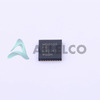
MD0105K6-G
Microchip Technology
IC INTERFACE SPECIALIZED 18DFN
MAX944ESD+T
Analog Devices Inc./Maxim Integrated
IC COMPARATOR 4 GEN PUR 14SOIC
176759-1
TE Connectivity AMP Connectors
CONN SOCKET 22-26AWG CRIMP TIN
SN74AHC08DR
Texas Instruments
IC GATE AND 4CH 2-INP 14SOIC
MMSZ5241B
Diotec Semiconductor
ZENER SOD-123 11V 0.5W 5%
FDMS7680
Fairchild Semiconductor
MOSFET N-CH 30V 14A/28A 8PQFN
AFE5812ZCF
Texas Instruments
IC AFE 8 CHAN 12/14BIT 135NFBGA
BZX84-C27
Nexperia USA Inc.
NOW NEXPERIA BZX84-C24 - ZENER D
ISL9203CRZR5220
Intersil
IC BATT CHG LI-ION 1CELL 10DFN
AEDS-9641-210
Broadcom Limited
ROTARY ENCODR OPTICAL 300 LPI
LMV331IDBVRG4
Texas Instruments
IC COMPARATOR 1 GEN PUR SOT23-5
LTC3851AEUD-1#TRPBF
Analog Devices Inc.
IC REG CTRLR BUCK 16QFN
S26KL256SDABHI020
Infineon Technologies
IC FLASH 256MBIT PAR 24FBGA
AD9740WARUZRL7
Analog Devices Inc.
IC DAC 10BIT A-OUT 28TSSOP
AP1084D33L-13
Diodes Incorporated
IC REG LDO 3.3V 5A TO-252 -

SF-1206F250-2
Bourns Inc.
FUSE BOARD MOUNT 2.5A 32VDC 1206
VJ1812Y224KXCAT
Electro-Films (EFI) / Vishay
CAP CER 0.22UF 200V X7R 1812
FOD617B3S
onsemi
OPTOISOLATOR 5KV TRANSISTOR 4SMD
TC6501P105VCTTR
Microchip Technology
THERMOSTAT 105DEG ACT LO SOT23-5
NCP562SQ25T1
onsemi
IC REG LINEAR 2.5V 80MA SC82AB
U77-A1113-1001
Amphenol ICC (Commercial Products)
CONN SFP CAGE SLD R/A
CY2544C011
Infineon Technologies
TSBU
VI-26R-CV-01
Vicor Corporation
VI-26R-CV-01 300V/7.5V 150W
STGWT30V60DF
STMicroelectronics
IGBT 600V 60A 258W TO3P-3
MK22DX256VLF5
NXP USA Inc.
IC MCU 32BIT 256KB FLASH 48LQFP
PAC1932T-I/J6CX
Microchip Technology
IC CURRENT MONITOR 1% 16WLCSP
M30280FAHP#U9B
Renesas Electronics America Inc
IC MCU 16BIT 96KB FLASH 80LQFP
TWL6030B1ADCMRR
Texas Instruments
TWL6030B1ADCMRR
VS-26MT40
Vishay General Semiconductor - Diodes Division
BRIDGE RECT 3PHASE 400V 25A D-63
LM239DR2
onsemi
IC COMP QUAD SGL SUPPLY 14SOIC
MCMA140P1200TA
IXYS
SCR MODULE 1.2KV 140A TO240AA
XC6221B302GR-G
Torex Semiconductor Ltd
IC REG LINEAR 3V 200MA 4USP
NJM78L20UA-TE1
Nisshinbo Micro Devices Inc.
IC REG LINEAR 20V 100MA SOT89