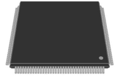
XC2C256-7TQ144C CPLD: Pinout, Features, Programming and Datasheet Guide
In this guide, you’ll get a clear look at the XC2C256-7TQ144C, a low-power CPLD from Xilinx’s CoolRunner-II family (now AMD). You’ll learn about its pin configuration, CAD models, and main features like logic capacity, I/O options, voltage support, and power-saving functions. We’ll also walk through its architecture, I/V curve, and specifications, followed by applications, similar parts, programming steps, advantages and disadvantages, packaging details, and manufacturer information so you can understand exactly how this device fits into your projects.Catalog
What is the XC2C256-7TQ144C?
The XC2C256-7TQ144C is a low-power CPLD (Complex Programmable Logic Device) from Xilinx’s CoolRunner-II family, now part of AMD. It features 256 macrocells and comes in a 144-pin TQFP package, designed for fast, deterministic operation with minimal power consumption. Operating on a 1.8 V core, it offers reliable performance in a compact form factor and is well-suited for designs requiring instant-on capability and efficient logic implementation. As part of the versatile CoolRunner-II series, it benefits from a proven architecture and broad design compatibility.
Looking for XC2C256-7TQ144C? Contact us to check current stock, lead time, and pricing.
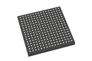
XC2C256-7TQ144C Pin-Out Diagram
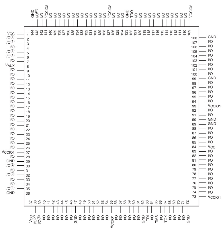
The XC2C256-7TQ144C pin-out diagram shows how the 144 pins are arranged for power, ground, JTAG, and user-programmable I/O functions. Most pins are I/O, which can be configured as inputs or outputs, and are evenly distributed to support flexible routing. VCC, VCCIO1, VCCIO2, VAUX, and GND pins are placed around the package to provide stable power distribution and multiple I/O voltage options. The JTAG pins (TDI, TDO, TMS, TCK) are grouped together for easy in-system programming and testing.
XC2C256-7TQ144C CAD Models
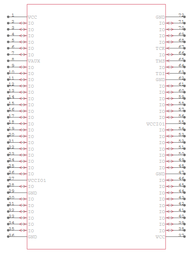
XC2C256-7TQ144C Symbol
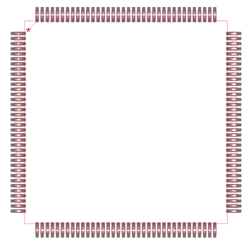
XC2C256-7TQ144C Footprint
XC2C256-7TQ144C 3D Model
XC2C256-7TQ144C Features
• Device Type and Family
The XC2C256-7TQ144C is a Complex Programmable Logic Device (CPLD) that belongs to the CoolRunner-II family developed by Xilinx (now AMD). It is designed for low power consumption while maintaining fast, deterministic logic performance, making it ideal for control logic and interfacing applications.
• Logic Capacity
This device contains 256 macrocells, which are the programmable logic resources in the CPLD. These macrocells can be configured to implement various combinational and sequential logic functions, giving moderate capacity for control, glue logic, and bus interfaces.
• Logic Blocks (Function Blocks)
It integrates 16 function blocks that organize and manage groups of macrocells. Each block provides local interconnect and product-term resources, allowing flexible logic implementation and efficient routing within the device.
• User I/O Pins
The XC2C256-7TQ144C offers up to 118 user-configurable I/O pins in its TQFP-144 package. This high pin count enables the device to interface with multiple subsystems simultaneously, making it suitable for complex board-level designs.
• Core Voltage (VCC)
The core operates at a nominal 1.8 V (1.7 V to 1.9 V range), which helps reduce power consumption compared to older 5 V CPLDs. This lower voltage is useful in modern mixed-voltage digital systems.
• Multi-Voltage I/O Support
The I/O banks support multiple voltage standards including 1.5 V, 1.8 V, 2.5 V, and 3.3 V. This flexibility allows the CPLD to directly interface with components operating at different voltage levels without external level shifters.
• High-Speed Operation
With a typical pin-to-pin propagation delay of around 5.7 ns (speed grade “-7”), the device delivers fast, deterministic performance. This makes it suitable for timing-critical applications such as address decoding, bus arbitration, and control.
• Low Power Consumption
The CoolRunner-II series is known for extremely low standby currents, often in the microamp range. This low static power, combined with dynamic power-saving features, allows the XC2C256-7TQ144C to be used effectively in battery-powered or always-on systems.
• DataGATE Technology
This feature enables to gate off unused inputs, preventing unnecessary toggling and reducing dynamic power consumption. It is valuable in applications where certain signals are inactive for long periods.
• In-System JTAG Programming
The device supports IEEE 1149.1 (JTAG) and IEEE 1532 for in-system programming. This means the CPLD can be configured, tested, and reprogrammed without removing it from the board, simplifying development and updates.
• Advanced Clocking Structure
XC2C256-7TQ144C includes multiple global clocks, clock dividers, and dual-edge triggered registers. It also provides global set/reset and local clocking per macrocell, giving flexible control over timing and synchronization.
• Schmitt-Trigger Inputs
Selected input pins can be configured as Schmitt triggers to improve noise immunity. This is useful for handling slow or noisy input signals without adding external conditioning circuitry.
• Flexible Output Features
The outputs support three-state operation, slew rate control, bus-hold, open-drain configurations, and optional pull-ups. These options make it easy to adapt the CPLD to various bus standards and external load conditions.
• Advanced Interconnect Matrix (AIM)
An Advanced Interconnect Matrix efficiently links function blocks, providing full product-term routing across the device. This improves logic placement flexibility and helps maintain predictable timing performance.
CoolRunner-II CPLD Architecture
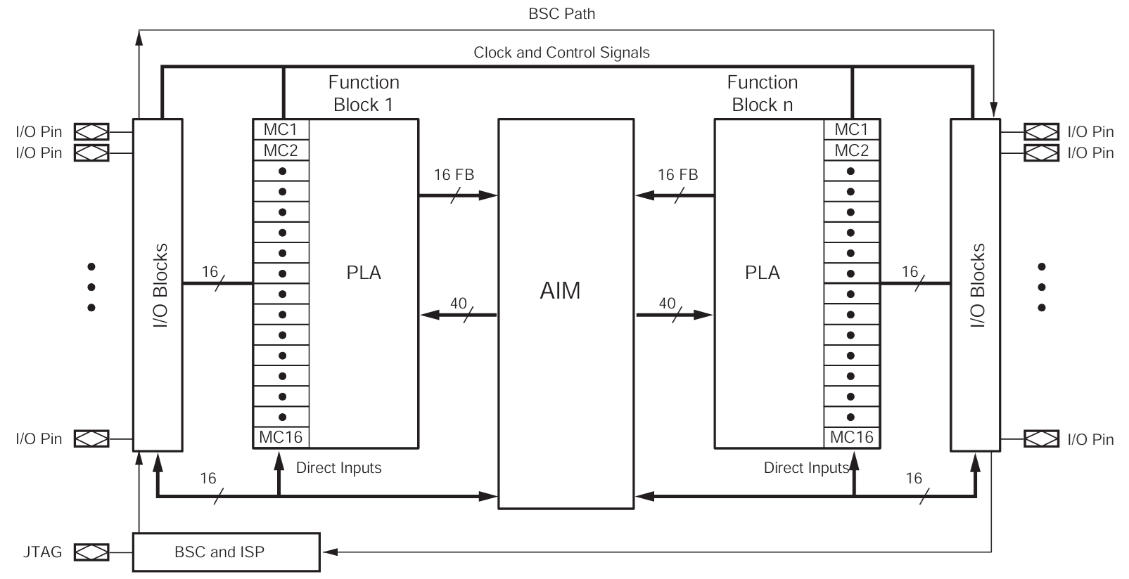
The CoolRunner-II CPLD architecture of the XC2C256-7TQ144C is built around Function Blocks, I/O Blocks, and an Advanced Interconnect Matrix (AIM). Each function block contains macrocells and a programmable logic array (PLA) that implement user-defined logic, while the AIM efficiently routes signals between blocks. The I/O blocks interface the internal logic with external pins, and dedicated JTAG and BSC/ISP circuitry support in-system programming and testing. This structured and interconnected architecture enables fast, deterministic performance with low power consumption, making it ideal for control, interfacing, and glue logic in digital systems.
Typical I/V Curve for XC2C256
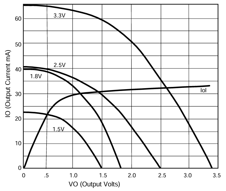
The Typical I/V Curve for the XC2C256-7TQ144C illustrates the relationship between output voltage (VO) and output current (IO) for different I/O supply voltages (1.5 V, 1.8 V, 2.5 V, and 3.3 V). As the supply voltage increases, the device can source or sink higher currents before the output voltage begins to drop significantly. This behavior is important for understanding the drive capability of the CPLD when interfacing with external components, ensuring signal levels remain valid under load. Many use this curve to select appropriate I/O voltages and ensure reliable operation in applications that demand specific current-driving strengths.
XC2C256-7TQ144C Specifications
|
Type |
Parameter |
|
Manufacturer |
AMD/Xilinx |
|
Series |
CoolRunner II |
|
Packaging |
Tray |
|
Part Status |
Obsolete |
|
Programmable Type |
In System Programmable |
|
Delay Time tpd(1) Max |
6.7 ns |
|
Voltage Supply – Internal |
1.7 V ~ 1.9 V |
|
Number of Logic Elements/Blocks |
16 |
|
Number of Macrocells |
256 |
|
Number of Gates |
6000 |
|
Number of I/O |
118 |
|
Operating Temperature |
0 °C ~ 70 °C (TA) |
|
Mounting Type |
Surface Mount |
|
Package / Case |
144-LQFP |
|
Supplier Device Package |
144-TQFP (20×20) |
|
Base Product Number |
XC2C256 |
XC2C256-7TQ144C Applications
1. Glue Logic and Interface Bridging
The XC2C256-7TQ144C is ideal for implementing glue logic, which connects and coordinates signals between different digital components. It can handle functions like address decoding, bus arbitration, and protocol translation, enabling smooth communication between microcontrollers, memory, sensors, and other peripherals. Its predictable timing and fast pin-to-pin delays ensure reliable interfacing even in complex board designs.
2. Low-Power and Battery-Operated Devices
Thanks to its Fast Zero Power (FZP) technology and very low standby current, this CPLD is highly suitable for portable and battery-powered electronics. It can remain powered continuously while consuming minimal energy, making it perfect for always-on control or monitoring circuits. You can reduce power usage further with features like DataGATE, which minimizes dynamic switching when inputs are inactive.
3. Control Logic and Sequencing
The device excels at implementing finite state machines, timing control, and signal sequencing required in many embedded systems. Its deterministic, non-volatile architecture allows the control logic to become active immediately after power-up without configuration delays. This makes it a strong choice for reset logic, handshaking circuits, and other time-critical control tasks.
4. Embedded System Support and Peripheral Logic
In embedded designs, the XC2C256-7TQ144C can act as a customizable support chip, implementing specialized interfaces or extending a microcontroller’s capabilities. It can handle communication protocols like SPI, I²C, or UART, generate chip selects, or manage interrupt routing. By offloading these functions from the CPU, it simplifies firmware development and improves overall system performance.
XC2C256-7TQ144C Similar Parts
|
Specification |
XC2C256-7TQ144C |
XC2C256-7TQ144I |
XC2C256-7TQG144I |
XC2C256-7VQ100C |
XC2C256-7VQG100C |
XC2C256-6TQ144C |
|
Device Family |
CoolRunner-II CPLD |
CoolRunner-II CPLD |
CoolRunner-II CPLD |
CoolRunner-II CPLD |
CoolRunner-II CPLD |
CoolRunner-II CPLD |
|
Logic Density (Macrocells) |
256 |
256 |
256 |
256 |
256 |
256 |
|
Package Type |
TQFP-144 |
TQFP-144 |
TQFP-144 (Pb-free) |
VQFP-100 |
VQFP-100 (Pb-free) |
TQFP-144 |
|
Speed Grade |
-7 |
-7 |
-7 |
-7 |
-7 |
-6 (faster) |
|
Temperature Range |
Commercial (0 – 70 °C) |
Industrial (-40 – 85 °C) |
Industrial (-40 – 85 °C) |
Commercial (0 – 70 °C) |
Commercial (0 – 70 °C) |
Commercial (0 – 70 °C) |
|
I/O Pin Count |
118 |
118 |
118 |
80 |
80 |
118 |
|
Core Voltage (VCC) |
1.8 V |
1.8 V |
1.8 V |
1.8 V |
1.8 V |
1.8 V |
|
I/O Voltage Support |
1.5 V – 3.3 V |
1.5 V – 3.3 V |
1.5 V – 3.3 V |
1.5 V – 3.3 V |
1.5 V – 3.3 V |
1.5 V – 3.3 V |
|
Compliance / Pb-Free |
Standard |
Standard |
Pb-Free / RoHS |
Standard |
Pb-Free / RoHS |
Standard |
|
Differences |
Baseline commercial version |
Industrial temp version |
Industrial + Pb-free version |
Smaller package, fewer I/O |
Pb-free smaller version |
Faster timing version |
XC2C256-7TQ144C Programming Steps
Programming the XC2C256-7TQ144C is a straightforward process that involves preparing your design, generating the programming file, and loading it into the CPLD through JTAG. By following each step carefully, you can ensure a successful configuration and proper device operation on your board.
1. Design and Synthesize
You start by writing your logic design using HDL (VHDL or Verilog) or schematic entry. After completing the design, you run the synthesis process, which converts your logic into the device’s internal structure of macrocells and interconnects. This step ensures your design is compatible with the XC2C256 architecture and ready for implementation.
2. Place & Route / Implementation (Fitting)
Next, you perform place and route, also known as fitting, which assigns your synthesized logic to actual physical macrocells and routing resources inside the CPLD. The tool checks timing constraints, resolves resource usage, and optimizes paths to meet the performance of your design. This ensures the circuit will run reliably once programmed into the device.
3. Generate Programming File
Once the implementation is complete, you generate the programming file (BIT, JAM, or SVF format) that contains the exact configuration data for the device. This file represents how each macrocell, interconnect, and I/O is set up to implement your logic. Having this file ready is needed before moving on to the actual device programming.
4. JTAG / In-System Programming
Finally, you connect the device to your PC using a JTAG programming cable and open the Xilinx iMPACT tool (or equivalent). You then load the generated programming file and download it to the XC2C256-7TQ144C through the JTAG pins (TDI, TDO, TCK, TMS). Once the process is complete, the CPLD immediately starts operating with your programmed logic, without requiring a power cycle or external configuration memory.
XC2C256-7TQ144C Advantages and Disadvantages
Advantages
• Very low standby power, ideal for battery-powered designs.
• Instant-on operation with no configuration delay.
• Predictable timing for easier design closure.
• Replaces multiple discrete logic chips, saving space and cost.
• Supports multiple I/O voltages without external level shifters.
Disadvantages
• Limited logic capacity compared to larger CPLDs or FPGAs.
• No built-in DSP, RAM, or high-speed transceivers.
• Becoming obsolete, making future sourcing harder.
• Lower performance ceiling for high-speed applications.
• Less routing flexibility for complex or irregular designs.
XC2C256-7TQ144C Packaging Dimensions
|
Type |
Parameter |
|
Package Type |
TQFP-144 |
|
Package Body Size |
20 mm × 20 mm |
|
Lead Pitch |
0.5 mm |
|
Number of Pins |
144 |
|
Package Height (Max) |
1.4 mm |
|
Package Thickness (Nominal) |
1.0 mm |
|
Lead Length |
0.45 mm ~ 0.75 mm |
|
Lead Width |
0.17 mm ~ 0.27 mm |
|
Mounting Type |
Surface Mount |
|
Supplier Device Package |
144-TQFP (20 × 20) |
XC2C256-7TQ144C Manufacturer
The XC2C256-7TQ144C is manufactured by Xilinx, a leading company in programmable logic solutions. Xilinx is widely recognized for pioneering FPGA and CPLD technologies, providing reliable and high-performance devices for industrial, commercial, and consumer applications. Today, Xilinx operates as part of AMD, continuing to deliver advanced programmable logic products with strong long-term support and innovation.
Conclusion
The XC2C256-7TQ144C stands out for its low power consumption, fast deterministic performance, and multi-voltage I/O flexibility, making it a reliable choice for modern digital designs. Its balanced combination of 256 macrocells, 118 I/O pins, and advanced interconnect architecture supports a wide range of control, interfacing, and glue logic functions. With support for in-system programming, DataGATE power-saving features, and robust I/O configurations, it integrates smoothly into embedded systems and mixed-voltage environments.
Datasheet PDF
XC2C256-7TQ144C Datasheets:
About us
ALLELCO LIMITED
Read more
Quick inquiry
Please send an inquiry, we will respond immediately.
Frequently Asked Questions [FAQ]
1. Does the XC2C256-7TQ144C require external configuration memory?
No. One of its advantages is instant-on operation. The configuration is stored internally, so it powers up ready to run without any external PROM or Flash memory.
2. What programming tools are compatible with XC2C256-7TQ144C?
You can program the device using Xilinx iMPACT software with a JTAG programming cable. Many also use compatible third-party JTAG programmers, but make sure they support IEEE 1149.1/1532 standards.
3. Can the XC2C256-7TQ144C replace multiple discrete logic ICs in your design?
Yes. With its 256 macrocells and flexible I/O, this CPLD can integrate several glue logic and control functions into one device, helping you reduce board space and component count.
4. Is the XC2C256-7TQ144C suitable for low-power battery applications?
Yes. Thanks to its Fast Zero Power (FZP) technology and very low standby current, it’s ideal for always-on circuits, portable devices, and power-sensitive embedded systems.
5. Can you use the XC2C256-7TQ144C for high-speed signal processing?
It’s not designed for high-speed DSP or transceiver tasks. While it delivers fast pin-to-pin delays, it’s best suited for control, interfacing, and timing logic, not complex data processing.
EP2S60F672C4 FPGA: Features, Applications, Programming & Datasheet Guide
on October 4th
EPM3256AFC256-7 CPLD Overview: Features, Pinout, Programming
on October 3th
Popular Posts
-

Complex Instruction Set Computers: How They Changed Computing?
on April 17th 147712
-

USB-C Pinout and Features
on April 17th 111691
-

Using Xilinx Unified Simulation Primitives: A Comprehensive Guide to FPGA Design and Simulation
on April 17th 111316
-

Power Supply Voltages in Electronics: Meaning of VCC, VDD, VEE, VSS, and GND
on April 17th 83590
-

RJ45 Connector Guide: Pinout, Wiring, Cable Types, and Uses
on January 1th 79242
-

The Ultimate Guide to Wire Color Codes in Modern Electrical Systems
The way our electrical systems use colors isn’t just for looks. Each wire color now indicates a specific function, making it easier to identify and handle electrical components correctly during ins...on January 1th 66758
-

Quality (Q) Factor: Equations and Applications
The quality factor, or 'Q', is important when checking how well inductors and resonators work in electronic systems that use radio frequencies (RF). 'Q' measures how well a circuit minimizes energy...on January 1th 62931
-

Purge Valve Guide: Function, Symptoms, Testing, and Replacement for Optimal Engine Performance
The purge valve is a key part of a car’s system that helps keep the air clean by managing fuel vapors before they can escape into the atmosphere. This not only helps the environment by reducing pol...on January 1th 62806
-

Achieving Peak Performance with the Maximum Power Transfer Theorem
The Maximum Power Transfer Theorem explains how energy from a source, such as a battery or generator, flows to a connected load. It shows the exact condition where the load receives the most power....on January 1th 54025
-

A23 Battery Specifications and Compatibility
The A23 battery is a small, cylinder-shaped battery with high voltage. Also called 23A, 23AE, or MN21, it runs at 12 volts and much higher than AA or AAA batteries. Its special design make...on January 1th 51955
HOT Part Number
-

NCV4275DSR4
onsemi
IC REG LINEAR 5V 450MA D2PAK-5
LM2576D2T-ADJR4G
onsemi
IC REG MULT CONFG ADJ 3A D2PAK-5
BA50JC5T
Rohm Semiconductor
IC REG LINEAR 5V 1.5A TO220FP
IRSF3031L
Infineon Technologies
IC PWR DRIVER N-CHAN 1:1 SOT223
74AHC00S14-13
Diodes Incorporated
IC GATE NAND 4CH 2-INP 14SO
TLP250(F)
Toshiba Semiconductor and Storage
OPTOISO 2.5KV 1CH GATE DRVR 8DIP
GRM022R71A121KA01L
Murata Electronics
CAP CER 120PF 10V X7R 01005
GALI-6+
Mini-Circuits
IC AMP CELLULAR 0HZ-4GHZ SOT89
SMCJ60A
Bourns Inc.
TVS DIODE 60VWM 96.8VC SMC
R1S-0505/H
Recom Power
DC DC CONVERTER 5V 1W
ADP7102ACPZ-1.8-R7
Analog Devices Inc.
IC REG LINEAR 1.8V 300MA 8LFCSP
L78L05ABZ-TR
STMicroelectronics
IC REG LINEAR 5V 100MA TO92-3
SRN6045-221M
Bourns Inc.
FIXED IND 220UH 600MA 1.18OHM SM
STPS340U
STMicroelectronics
DIODE SCHOTTKY 40V 3A SMB
APTGT25A120D1G
Microsemi Corporation
IGBT MODULE 1200V 40A 140W D1
CC0805KRX7RYBB471
YAGEO
CAP CER 470PF 250V X7R 0805
MAX3189EEUT+T
Analog Devices Inc./Maxim Integrated
IC DRIVER FULL 1/0 SOT23-6
UCC3803D
Texas Instruments
IC REG CTRLR MULT TOPOLOGY 8SOIC -
ADC0802LCN
Texas Instruments
IC ADC 8BIT SAR 20DIP
1808JA100KAT1A
KYOCERA AVX
CAP CER 10PF 4KV NP0 1808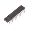
MAX185BCNG+
Analog Devices Inc./Maxim Integrated
IC ADC 12BIT HS 24-DIP
LTC4305CGN#TRPBF
Analog Devices Inc.
IC INTERFACE SPECIALIZED 16SSOP
TBU-CA065-050-WH
Bourns Inc.
SURGE SUPP TBU 50MA 650VIMP SMD
STSR2PMCD-TR
STMicroelectronics
IC GATE DRVR LOW-SIDE 8SO
RT0402BRE0751RL
YAGEO
RES SMD 51 OHM 0.1% 1/16W 0402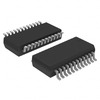
MT8888CN1
Microchip Technology
IC TELECOM INTERFACE 24SSOP
IXFK150N15
IXYS
MOSFET N-CH 150V 150A TO264AA
VI-HAMD-IM
Vicor Corporation
MOD HARMONIC ATTENUATOR
BYT60P-400
STMicroelectronics
DIODE ARRAY GP 400V 60A SOD93
MC9S08AC32CPUE
NXP USA Inc.
IC MCU 8BIT 32KB FLASH 64LQFP
SMD1812B010TF
YAGEO
GDT
ADG3233BRJ-REEL
Analog Devices Inc.
IC TRNSLTR BIDIRECTIONAL SOT23-8
AT27C040-15JI
Microchip Technology
IC EPROM 4MBIT PARALLEL 32PLCC
CSD87312Q3E
Texas Instruments
MOSFET 2N-CH 30V 27A 8VSON
MAX6775LTA+T
Analog Devices Inc./Maxim Integrated
IC BATT MON MULTI-CHEM 1CL 6UDFN
2220AC472KAT1A
KYOCERA AVX
CAP CER 4700PF 1KV X7R 2220 -
HF81GS-Z
Monolithic Power Systems Inc.
IC REG SWITCH CAP BLEED 8SOIC
LTC1694-1CS5#TRMPBF
Analog Devices Inc.
IC ACCELERATOR I2C 1CH TSOT23-5
GRM1555C1H271FA01D
Murata Electronics
CAP CER 270PF 50V C0G/NP0 0402
NX7002AK,215
NXP USA Inc.
SMALL SIGNAL FIELD-EFFECT TRANSI
M74HC688RM13TR
STMicroelectronics
IC COMPARATOR EQUALITY 8B 20SOIC
MVF50NN151CMK40
NXP USA Inc.
IC MCU 32BIT ROMLESS 364MAPBGA
08051A0R7CAT4A
KYOCERA AVX
CAP CER 0.7PF 100V NP0 0805
MCP73213-A6SI/MF
Microchip Technology
IC BATT CONTRL LI-ION 2CEL 10DFN
1N5828
GeneSiC Semiconductor
DIODE SCHOTTKY 40V 15A DO5
KA431D
Fairchild Semiconductor
IC VREF SHUNT ADJ 2% 8SOIC
ADG633YRUZ-REEL7
Analog Devices Inc.
IC SWITCH SPDT X 3 75OHM 16TSSOP
HZM18NB3TL-E
Renesas Electronics America Inc
DIODE ZENER
SST89E58RD2-40-C-NJE
Microchip Technology
IC MCU 8BIT 40KB FLASH 44PLCC
VRF152
Microchip Technology
MOSFET RF PWR N-CH 50V 150W M174
RK73B1HTTC182J
KOA Speer Electronics, Inc.
RES 1.8K OHM 5% 1/20W 0201
SI51211-A17AFMR
Skyworks Solutions Inc.
IC CLOCK GENERATOR 8TDFN
P6SMB47AT3G
Littelfuse Inc.
TVS DIODE 40.2VWM 64.8VC SMB
1N4007
Rectron USA
DIODE GEN PURP 1KV 1A DO41