EPM1270F256C4N MAX II CPLD Overview: Features, Specifications and Applications
In this article, you’ll learn about the EPM1270F256C4N, a mid-range CPLD from the MAX II family by Altera (now Intel). We’ll walk through what it is, the main features it offers, and how its block diagram and I/O banks make it flexible for different designs. You’ll also see its specifications, packaging, and CAD models. We’ll cover how it’s used in applications like bus bridging, PCI systems, configuration control, and power sequencing, as well as the steps to program it. Finally, we’ll look at its advantages, disadvantages, and some similar parts for comparison.Catalog
What is the EPM1270F256C4N?
The EPM1270F256C4N is a member of the MAX II family of Complex Programmable Logic Devices (CPLDs) developed by Altera, now part of Intel. It is a flash-based, non-volatile device designed for instant-on operation, eliminating the need for external configuration memory. Built on a 0.18 µm flash process, the device integrates logic resources, interconnects, and embedded flash memory into a compact solution that provides reliable performance with low power consumption. Positioned in the mid-range of the MAX II family, the EPM1270 offers around 1,270 logic elements, making it well-suited for projects that demand balanced capacity and efficiency without moving to the higher-end EPM2210. Like all MAX II devices, it benefits from in-system programmability through JTAG, MultiVolt I/O support, and on-chip user flash memory.
Looking for EPM1270F256C4N? Contact us to check current stock, lead time, and pricing.
EPM1270F256C4N CAD Models
EPM1270F256C4N Symbol
EPM1270F256C4N Footprint
EPM1270F256C4N 3D Model
EPM1270F256C4N Features
• Flash-Based, Non-Volatile Architecture
The device is built on a flash-based architecture, meaning it retains its configuration without the need for external memory. This allows for instant-on functionality, making it reliable for systems that must start operating immediately after power-up.
• Logic Capacity
The EPM1270F256C4N provides 1,270 logic elements (LEs) and about 980 macrocells, giving ample resources for implementing complex control logic. This makes it suitable for medium-density applications such as bus management, interface bridging, and embedded control.
• Programmable I/O Pins
It supports up to 212 programmable I/O pins, allowing flexible connectivity with a wide range of system interfaces. This versatility makes it easier to integrate with other devices that may use different voltage standards.
• User Flash Memory (UFM)
An integrated 8 Kbit UFM block enables storage of user-defined data, such as encryption keys or configuration parameters. This feature enhances system security and reduces the need for external EEPROMs.
• High-Speed Operation
With a maximum frequency of about 304 MHz and propagation delays as low as 6.2 ns, the device can handle time-critical logic functions. This ensures smooth performance in high-speed applications like signal processing and data communications.
• MultiVolt I/O Support
The CPLD supports multiple I/O standards from 1.5 V to 3.3 V, allowing it to interface seamlessly with devices operating at different voltages. This flexibility reduces the need for external level-shifting components.
• Power Efficiency
The device operates with typical supply currents around 55 mA, making it efficient compared to older CPLD families. Its low static power consumption helps in battery-powered and energy-sensitive systems.
• Advanced I/O Features
It includes built-in bus-hold resistors, programmable pull-ups, Schmitt-trigger inputs, and slew-rate control, which improve signal stability and noise tolerance. These features make the device robust when working in mixed-signal or noisy environments.
• In-System Programmability and Test
The EPM1270F256C4N supports JTAG-based programming and complies with IEEE 1532 for in-system programmability. Boundary-scan test support (IEEE 1149.1) ensures easier board testing and debugging during manufacturing.
• Hot-Socketing Support
This CPLD can be safely inserted or removed from a powered system without causing electrical damage. Hot-socketing simplifies maintenance and system upgrades without requiring power-down.
• Global Clock Networks
The device provides four global clock lines, enabling synchronized operation across its logic array. This ensures consistent timing and reliability in clock-intensive applications like counters, state machines, and high-speed controllers.
MAX II Block Diagram

The block diagram of the MAX II device, like the EPM1270F256C4N, shows how its main parts work together. At the center are Logic Array Blocks (LABs), which contain Logic Elements (LEs) that perform the actual programmable logic functions. Around the edges are I/O Elements (IOEs), which connect the internal logic to external pins for communication with other devices.
These parts are linked by the MultiTrack Interconnect, which acts like highways that quickly move signals between logic and I/O blocks. This setup makes the device fast, flexible, and reliable, allowing it to handle complex tasks while staying efficient in real-world applications.
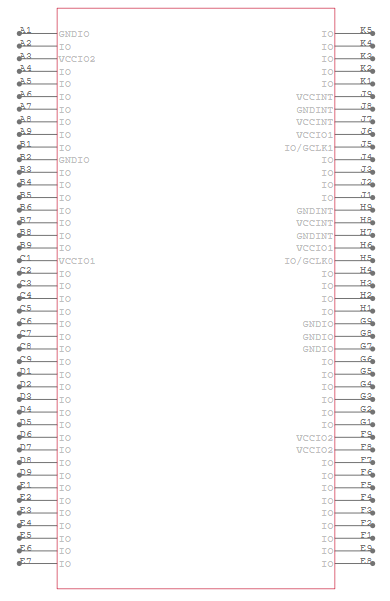
EPM1270 I/O Banks
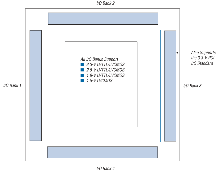
The I/O bank diagram of the EPM1270F256C4N shows how the device organizes its input and output connections. The chip is divided into four I/O banks, each surrounding the logic core and capable of supporting multiple voltage standards such as 3.3 V, 2.5 V, 1.8 V, and 1.5 V. This flexibility allows the device to interface with a wide range of external components, making it suitable for mixed-voltage systems without requiring extra level shifters.
One bank, shown as I/O Bank 3, also supports the 3.3 V PCI standard, enabling compatibility with legacy PCI-based designs. By separating pins into banks, you can assign different voltage levels to different groups, which enhances system integration and board design options. This structure is important because it gives the EPM1270F256C4N the ability to act as a central controller in complex systems, handling diverse signal standards while maintaining reliable performance.
EPM1270F256C4N Specifications
|
Type |
Parameter |
|
Manufacturer |
Altera/Intel |
|
Series |
MAX® II |
|
Packaging |
Tray |
|
Part Status |
Active |
|
Programmable Type |
In System Programmable |
|
Delay Time tpd(1) Max |
6.2 ns |
|
Voltage Supply - Internal |
2.5V, 3.3V |
|
Number of Logic Elements/Blocks |
1270 |
|
Number of Macrocells |
980 |
|
Number of I/O |
212 |
|
Operating Temperature |
0°C ~ 85°C (TJ) |
|
Mounting Type |
Surface Mount |
|
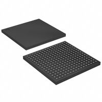
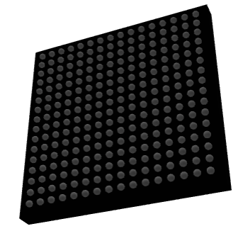
Package / Case |
256-BGA |
|
Supplier Device Package |
256-FBGA (17x17) |
|
Base Product Number |
EPM1270 |
EPM1270F256C4N Applications
1. Bus Bridging and Interface Bridging
The EPM1270F256C4N is widely used for bridging between different buses or communication protocols. With its flexible I/O banks supporting multiple voltage standards, it can connect modern devices to legacy systems without external converters. This makes it useful in mixed-technology environments where compatibility is needed.
2. PCI Bus Target or Repeater
This CPLD can act as a 32-bit PCI target at 66 MHz or serve as a repeater on backplane systems. By supporting the 3.3 V PCI standard, it ensures compliance with older designs while still operating efficiently in newer setups. This capability makes it a dependable choice in embedded boards and industrial controllers.
3. Bus Glue Logic and Address Decoding
Many often use the EPM1270F256C4N to implement glue logic that connects subsystems together. Its large number of logic elements can also handle address decoding, reducing the need for multiple discrete chips. This not only simplifies circuit design but also saves space and cost on the PCB.
4. Configuration Management and Flash Loader
The device is capable of managing FPGA configuration, often acting as a JTAG flash loader. It can store configuration data and directly program FPGAs, reducing external memory requirements. This makes it valuable in systems that require flexible or multi-device configuration handling.
5. Power-On Reset and Sequencing Control
The EPM1270F256C4N is well-suited for controlling reset signals and sequencing system power-up. It ensures that components initialize in the correct order, improving reliability during startup. Many use it for supervisory control to prevent errors caused by unstable power conditions.
6. I/O Expansion and Non-Volatile Storage
With over 200 I/O pins, the device can serve as an I/O expander in systems that need additional connectivity. Its built-in 8 Kbit User Flash Memory allows storage of parameters, configuration data, or encryption keys without external EEPROMs. This feature adds flexibility and security while reducing component count.
EPM1270F256C4N Similar Parts
|
Specification |
EPM1270F256C4N |
EPM1270F256C3N |
EPM1270F256C5N |
EPM1270F256I5N |
EPM1270F256C3ES |
EPM1270F256C4
|
|
Logic Elements (LEs) |
1,270 |
1,270 |
1,270 |
1,270 |
1,270 |
1,270 |
|
Macrocells |
~980 |
~980 |
~980 |
~980 |
~980 |
~980 |
|
I/O Pins |
Up to 212 |
Up to 212 |
Up to 212 |
Up to 212 |
Up to 212 |
Up to 212 |
|
User Flash Memory (UFM) |
8 Kbits |
8 Kbits |
8 Kbits |
8 Kbits |
8 Kbits |
8 Kbits |
|
Package |
256-FBGA |
256-FBGA |
256-FBGA |
256-FBGA |
256-FBGA |
256-FBGA |
|
Speed Grade |
C4 (standard) |
C3 (faster) |
C5 (higher) |
I5 (industrial) |
C3ES (faster) |
C4 (standard) |
|
Max Freq. (MHz) |
~304 |
~304 |
~304 |
~304 |
~304 |
~304 |
|
Propagation Delay |
~6.2 ns |
~6.2 ns |
~6.2 ns |
~6.2 ns |
~6.2 ns |
~6.2 ns |
|
Temp. Range |
0 to 70 °C |
0 to 70 °C |
0 to 85 °C |
–40 to +85 °C |
0 to 70 °C |
0 to 70 °C |
|
Use Case Strength |
General |
Higher speed |
Industrial/Hi |
Rugged/Harsh |
Dev/Test fast |
Equivalent alt |
EPM1270F256C4N Programming Steps
Before you can use the EPM1270F256C4N, you need to program it with your design. The process is straightforward if you follow each step carefully using the proper tools and software.
1. Prepare Your Tools and Hardware Connection
You begin by setting up the hardware environment. Connect your CPLD board to a PC using a compatible JTAG programmer, such as a USB-Blaster or ByteBlaster II cable. Ensure that the device has stable power and the JTAG pins (TDI, TDO, TCK, and TMS) are correctly connected. This makes sure your system is ready for communication before programming.
2. Generate the Programming File
Next, you use the Quartus II software to compile your design and create a programming file. The common file format is POF (Programmer Object File), but you may also create JAM (.jam) or JBC (.jbc) files if you need them for automated or embedded programming. By generating this file, you need package your logic design so it can be loaded into the CPLD.
3. Configure the Quartus Programmer
Open the Quartus Programmer tool and choose your connected JTAG hardware in the setup options. Then load the POF, JAM, or JBC file you created in the previous step. The software will automatically detect the CPLD device on the JTAG chain, and you must select it for programming. This step prepares the tool to communicate directly with the chip.
4. Program the Configuration Flash Memory (CFM)
Now you can begin programming the device. The Quartus Programmer transfers your design into the device’s Configuration Flash Memory (CFM), which permanently stores your logic. Once programmed, the device will automatically load the design at power-up, taking advantage of its instant-on flash architecture. This ensures your system starts operating immediately after reset or power cycling.
5. Enable Real-Time In-System Programming (Optional)
If you want to update the CPLD without stopping its current operation, you can enable real-time ISP. This feature allows you to program a new design image into flash memory while the device continues running. The new design will only take effect after the next reset or power cycle. It’s especially helpful in systems that must remain operational during updates.
6. Apply ISP Clamp if Needed (Optional)
During programming, you may need certain I/O pins to stay stable. In such cases, you can use the ISP Clamp feature to force pins into high, low, or hold states during programming. This prevents disturbances on signals while the chip is being updated. It ensures system safety when programming in live environments.
7. Use Jam/JBC Files for Automation (Optional)
For embedded applications or automated test setups, you can use JAM or JBC files instead of directly loading a POF. These files are script-based and allow you to automate programming tasks through external controllers. By doing this, you can manage CPLD updates in production lines or field systems without needing Quartus on a PC.
8. Program the User Flash Memory (Optional)
The device also includes an 8 Kbit User Flash Memory (UFM) block for non-volatile user data. You can program this separately to store items like configuration settings, encryption keys, or calibration data. Since UFM is independent of the main logic, you can update it without affecting the programmed design. This makes the chip useful for security and system customization.
9. Verify and Test the Device
After programming, it’s important to verify the process. Quartus automatically performs a verification check, but you should also test your system logic to confirm it behaves as expected. The design will begin running immediately after programming, giving you instant feedback. This step ensures reliability before moving into full deployment.
10. Reconfigure or Update as Needed
Over time, you may need to improve or change your design. To do this, simply regenerate a new POF in Quartus and repeat the programming process. You can also use ISP or JAM scripts for smoother updates without system downtime. This flexibility makes the EPM1270F256C4N practical for evolving projects.
EPM1270F256C4N Advantages and Disadvantages
Advantages
• Low cost compared to older CPLDs and similar devices.
• Very low power consumption, ideal for efficient systems.
• Higher performance and density than previous MAX families.
• Non-volatile, instant-on startup without external memory.
• Reduces external components, saving PCB space and cost.
Disadvantages
• Limited logic capacity compared to modern FPGAs.
• Lacks advanced blocks like DSPs or high-speed transceivers.
• Higher per-unit cost than ASICs at very high volumes.
• Requires HDL tools and programming knowledge.
• Fixed architecture limits flexibility in complex routing.
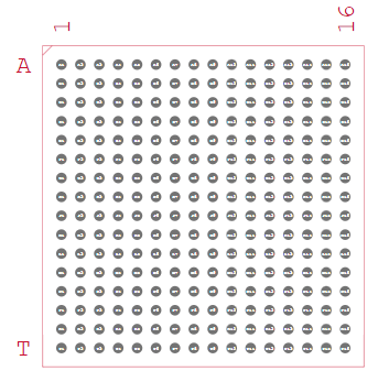
EPM1270F256C4N Packaging Dimensions
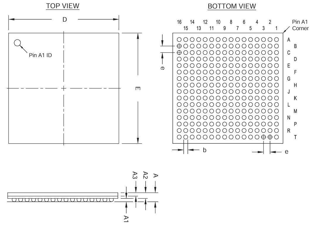
|
Type |
Parameter |
|
Package Type |
256-FBGA (17 × 17 mm) |
|
Dimension D (Body) |
17.0 mm |
|
Dimension E (Body) |
17.0 mm |
|
Ball Pitch (e) |
1.0 mm |
|
Ball Diameter (b) |
0.60 mm |
|
Overall Height (A) |
1.70 mm (max) |
|
Standoff Height (A1) |
0.25 mm (min) |
|
Package Thickness (A2) |
1.35 mm (typ) |
|
Substrate Thickness(A3) |
0.25 mm (typ) |
|
Pin A1 Identifier |
Corner Mark (Top View) |
EPM1270F256C4N Manufacturer
The EPM1270F256C4N is manufactured by Altera, a company recognized for its leadership in programmable logic devices, particularly CPLDs and FPGAs. Founded in 1983, Altera became a pioneer in programmable semiconductor technology and built a strong reputation for delivering innovative, cost-efficient, and high-performance logic solutions. In 2015, Altera was acquired by Intel Corporation, integrating its product lines into Intel’s Programmable Solutions Group. Today, the MAX II family, which includes the EPM1270F256C4N, continues to be supported and distributed under the Intel brand, combining Altera’s legacy of programmable logic expertise with Intel’s global scale, advanced semiconductor manufacturing, and long-term reliability in supply.
Conclusion
The EPM1270F256C4N offers instant-on, flash-based programmability with balanced logic capacity, low power use, and broad I/O voltage support. It provides reliable operation for bridging, glue logic, system control, and I/O expansion while including options like user flash memory and in-system programmability. Although it has fewer resources than modern FPGAs and lacks advanced functions like DSP blocks, it makes up for this with lower cost, simplicity, and reduced need for extra components. Overall, it is a strong choice for embedded and industrial systems that need efficiency, flexibility, and dependable performance.
Datasheet PDF
EPM1270F256C4N Datasheets:
About us
ALLELCO LIMITED
Read more
Quick inquiry
Please send an inquiry, we will respond immediately.
Frequently Asked Questions [FAQ]
1. Can the EPM1270F256C4N be used in battery-powered systems?
Yes, with its low static power consumption and efficient flash-based design, it is well-suited for portable or battery-powered applications that require reliability without draining energy.
2. Does the EPM1270F256C4N require external memory for operation?
No, one of its main advantages is its flash-based non-volatile design, which removes the need for an external configuration memory, reducing component count and board space.
3. Is the EPM1270F256C4N compatible with legacy PCI systems?
Yes, the device supports the 3.3 V PCI standard, allowing it to connect with older PCI-based systems while still maintaining compatibility with modern mixed-voltage environments.
4. Can the EPM1270F256C4N be updated while running in a system?
Yes, it supports in-system programming (ISP), meaning updates can be loaded into flash memory while the device continues operating, minimizing system downtime.
5. What makes the EPM1270F256C4N more reliable than older CPLDs?
Its instant-on flash design, advanced I/O features like bus-hold resistors and Schmitt-trigger inputs, and hot-socketing support all contribute to higher reliability and safer integration.
LFEC3E-3Q208C FPGA Overview: Features, Applications, Programming, and Specifications
on August 28th
TMS320C6421ZWT5 DSP Overview: Features, Alternatives, Specifications, and Applications
on August 26th
Popular Posts
-

Complex Instruction Set Computers: How They Changed Computing?
on April 18th 147778
-

USB-C Pinout and Features
on April 18th 112038
-

Using Xilinx Unified Simulation Primitives: A Comprehensive Guide to FPGA Design and Simulation
on April 18th 111352
-

Power Supply Voltages in Electronics: Meaning of VCC, VDD, VEE, VSS, and GND
on April 18th 83797
-

RJ45 Connector Guide: Pinout, Wiring, Cable Types, and Uses
on January 1th 79603
-

The Ultimate Guide to Wire Color Codes in Modern Electrical Systems
The way our electrical systems use colors isn’t just for looks. Each wire color now indicates a specific function, making it easier to identify and handle electrical components correctly during ins...on January 1th 66979
-

Purge Valve Guide: Function, Symptoms, Testing, and Replacement for Optimal Engine Performance
The purge valve is a key part of a car’s system that helps keep the air clean by managing fuel vapors before they can escape into the atmosphere. This not only helps the environment by reducing pol...on January 1th 63113
-

Quality (Q) Factor: Equations and Applications
The quality factor, or 'Q', is important when checking how well inductors and resonators work in electronic systems that use radio frequencies (RF). 'Q' measures how well a circuit minimizes energy...on January 1th 63047
-

Achieving Peak Performance with the Maximum Power Transfer Theorem
The Maximum Power Transfer Theorem explains how energy from a source, such as a battery or generator, flows to a connected load. It shows the exact condition where the load receives the most power....on January 1th 54097
-

A23 Battery Specifications and Compatibility
The A23 battery is a small, cylinder-shaped battery with high voltage. Also called 23A, 23AE, or MN21, it runs at 12 volts and much higher than AA or AAA batteries. Its special design make...on January 1th 52198
HOT Part Number
-

7008L20PFGI
Renesas Electronics America Inc
IC SRAM 512KBIT PARALLEL 100TQFP
ATF1502AS-7AX44
Microchip Technology
IC CPLD 32MC 7.5NS 44TQFP
CD4047BNSR
Texas Instruments
IC MULTIVIBRATOR 80NS 14SOP
IR2130JPBF
Infineon Technologies
IC GATE DRVR HALF-BRIDGE 44PLCC
10M50DAF484I7G
Intel
IC FPGA 360 I/O 484FBGA
7000AT18A1600E-AEC
Johanson Technology
RF ANT 7GHZ CER PATCH SOLDER SMD
MAX4514ESA
Analog Devices Inc./Maxim Integrated
IC SWITCH SPST-NOX1 20OHM 8SOIC
SN74HCT573PW
Texas Instruments
IC LATCH OCT TRANSP D 20-TSSOP
AD8145WYCPZ-R7
Analog Devices Inc.
IC INTERFACE SPECIALIZED 32LFCSP
EMK212BB7106KG-T
Taiyo Yuden
CAP CER 10UF 16V X7R 0805
SI4467DY
Fairchild Semiconductor
P-CHANNEL POWER MOSFET
MAX1239KEEE+T
Analog Devices Inc./Maxim Integrated
IC ADC 12BIT SAR 16QSOP
SMDJ10CA
Taiwan Semiconductor Corporation
TVS DIODE 10VWM 17VC DO214AB
ICL7662EPA
Analog Devices Inc./Maxim Integrated
ICL7662 CMOS VOLTAGE CONVERTER
FMMD914TA
Diodes Incorporated
DIODE GEN PURP 75V 75MA SOT23-3
6118
Pomona Electronics
KIT LEAD FLUKE 860 SERIES
OPA2735AIDGKR
Texas Instruments
IC OPAMP ZERO-DRIFT 2CIRC 8VSSOP
ATR0625P-PYQW
Microchip Technology
IC GPS BASE PROCESSOR 56-QFN -

ZTX968STZ
Diodes Incorporated
TRANS PNP 12V 4.5A E-LINE
P0420NL
Pulse Electronics
CMC 3.3A 2LN SMD
LEM2520T8R2J
Taiyo Yuden
FIXED IND 8.2UH 160MA 3.05OHM SM
BAV19TR
Fairchild Semiconductor
DIODE GEN PURP 120V 200MA DO35
PIC16C765-I/L
Microchip Technology
IC MCU 8BIT 14KB OTP 44PLCC
RT8241EZQW
Richtek USA Inc.
IC REG CTRLR BUCK 12WQFN
CGA5H2X8R2A104K115AD
TDK Corporation
CAP CER 0.1UF 100V 1206 EPOXY
DS2502-E48+
Analog Devices Inc./Maxim Integrated
IC EPROM 1KBIT 1-WIRE TO92-3
SML-D13FWT86
Rohm Semiconductor
LED GREEN DIFFUSED 0603 SMD
1206YC683MAT2A
KYOCERA AVX
CAP CER 0.068UF 16V X7R 1206
PIC16F1519-I/MV
Microchip Technology
IC MCU 8BIT 28KB FLASH 40UQFN
60R065XPR
Littelfuse Inc.
PTC RESET FUSE 60V 650MA RADIAL
742792643
Würth Elektronik
FERRITE BEAD 470 OHM 0603 1LN
MC68020RC16E
NXP USA Inc.
IC MPU M680X0 16MHZ 114PGA
BYQ28X-200,127
WeEn Semiconductors
DIODE ARRAY GP 200V 10A TO220-3
IHLP2525CZER3R3M01
Vishay Dale
FIXED IND 3.3UH 6A 30 MOHM SMD
SY89872UMG
Microchip Technology
IC CLK BUFFER 1:3 2GHZ 16MLF
UDN2982A
Allegro MicroSystems
IC PWR DRIVER BIPOLAR 1:1 18DIP -
N74F244D
NXP USA Inc.
IC BUFFER NON-INVERT 5.5V 20SO
BCM48BF320T300A00
Vicor Corporation
DC DC CONVERTER 32V 300W
CC1206KRX7RABB471
YAGEO
CAP CER 470PF 200V X7R 1206
MC14175BDR2G
onsemi
IC FF D-TYPE SNGL 4BIT 16SOIC
BAS70-G
Comchip Technology
DIODE SCHOTTKY 70V 70MA SOT23-3
GCM1555C1H3R1CA16D
Murata Electronics
CAP CER 3.1PF 50V C0G/NP0 0402
PSMN013-30YLC,115
Nexperia USA Inc.
MOSFET N-CH 30V 32A LFPAK56
GRM1555C1E7R7DA01D
Murata Electronics
CAP CER 7.7PF 25V C0G/NP0 0402
C3216C0G1H392K060AA
TDK Corporation
CAP CER 3900PF 50V C0G 1206
GRM188R70J223KA01D
Murata Electronics
CAP CER 0.022UF 6.3V X7R 0603
LT6001CMS8#TRPBF
Analog Devices Inc.
IC OPAMP GP 2 CIRCUIT 8MSOP
LT3758IMSE#PBF
Analog Devices Inc.
IC REG CTRLR MULT TOP 10MSOP
MAX3948ETE+T
Analog Devices Inc./Maxim Integrated
IC LASER DRV 11.3GB 3.63V 16TQFN
BCM7406ZKFEB03G
Broadcom Limited
SOC DIGITAL GATEWAY
FJP5027OTU
onsemi
TRANS NPN 800V 3A TO220-3
STFI11N65M2
STMicroelectronics
MOSFET N-CH 650V 7A I2PAKFP
C358PB
Powerex Inc.
SCR 1200V 140A TO200AB
MDMA50P1200TG
IXYS
DIODE MODULE 1.2KV 50A TO240AA