Silicon Photonics Explained: How It Works, Components, Integration, and Applications
Silicon photonics lets you use light instead of electricity to move data inside and between chips. In this article, you will learn what it is, how it works, and the key components that make it function. You will also explore different integration methods, packaging developments, and where this technology is used. By the end, you will understand how it helps improve speed and efficiency in modern systems.Catalog
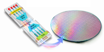
Figure 1. Silicon Photonics Overview
What Is Silicon Photonics?
Silicon photonics is a technology that uses light (photons) instead of electricity (electrons) to transmit data on silicon-based chips. It enables high-speed data communication by guiding light signals through microscopic structures fabricated using standard semiconductor processes. Unlike traditional electronic systems that rely on electrical current, silicon photonics uses optical signals, which can carry more data with less signal loss over distance. This approach allows faster and more efficient data transfer within and between devices. The core concept is based on replacing electron movement with photon propagation, reducing resistance-related limitations. As a result, silicon photonics is widely recognized as a key technology for next-generation high-speed communication systems.
Components of Silicon Photonics
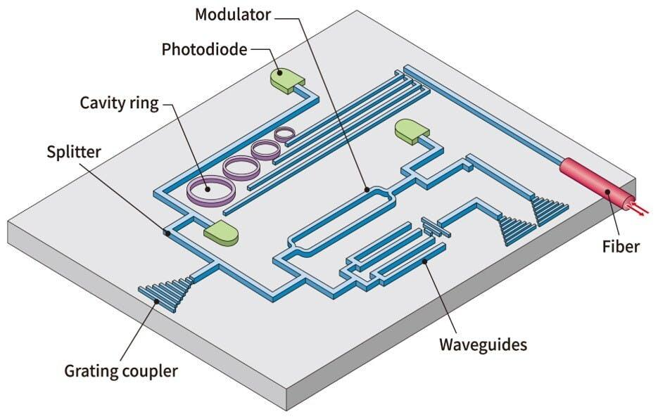
Figure 2. Silicon Photonic Components
• Waveguides
Waveguides are structures that guide light signals across the silicon chip. They confine and direct photons along predefined paths with minimal loss. These structures are typically made from silicon due to its high refractive index. They form the foundation for routing optical signals within the system.
• Modulator
A modulator encodes electrical data into an optical signal by altering the light properties. It can change the intensity, phase, or frequency of light to represent data. This process allows digital information to be transmitted using light. It plays a role in converting electrical signals into optical form.
• Photodetector (Photodiode)
A photodetector converts incoming light signals back into electrical signals. It detects optical power and generates a corresponding electrical current. This enables the system to interpret transmitted data at the receiving end. It is important for completing the optical communication process.
• Laser Source
The laser generates a coherent light signal used as the carrier for data transmission. It provides a stable and high-intensity optical source. This light is injected into the silicon photonic circuit. It acts as the starting point of the optical signal flow.
• Grating Coupler / Fiber Coupler
Couplers connect optical fibers to the silicon chip. They enable efficient transfer of light between external fibers and on-chip waveguides. These structures are designed to match optical modes for minimal loss. They serve as the interface between chip-level and system-level communication.
• Splitter
A splitter divides a single optical signal into multiple paths. It allows one input signal to be distributed across different channels. This is useful for parallel data transmission or signal routing. It helps increase system flexibility.
• Cavity Ring Resonator
A cavity ring is a circular waveguide structure used to filter or select specific wavelengths. It supports resonance at certain frequencies of light. This allows precise control of optical signals. It is often used in wavelength filtering and modulation.
How a Silicon Photonic Works?
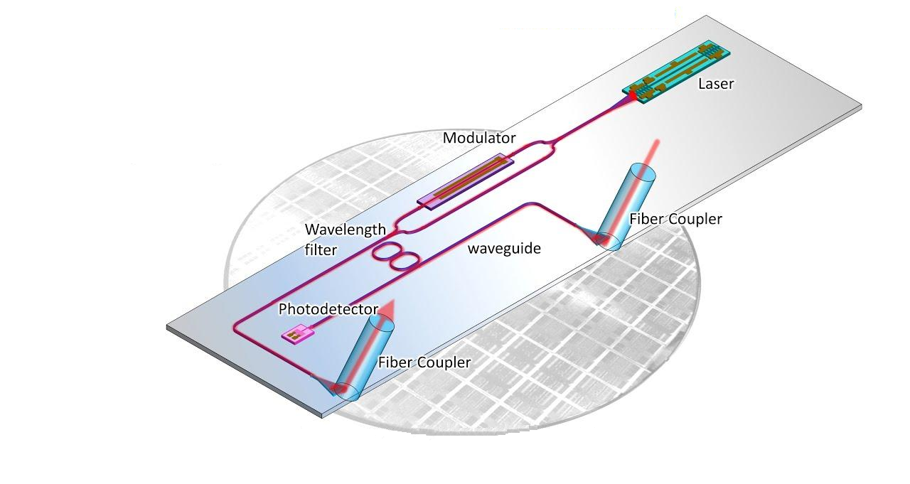
Figure 3. Silicon Photonic Working Principle
Silicon photonics operates by first generating a light signal that acts as a carrier for data. This light is then modified to represent information by encoding electrical signals into optical form. Once encoded, the optical signal is directed through microscopic pathways across the chip. These pathways allow the signal to travel efficiently without the resistance typically found in electrical systems. The transmission process ensures that large amounts of data can move quickly across short or long distances.
After traveling through the chip, the optical signal reaches the receiving end where it is converted back into an electrical signal. This conversion allows electronic systems to process the transmitted data. The entire process involves a continuous flow from light generation to signal detection. Each stage ensures minimal signal loss and high data integrity. This step-by-step flow enables high-speed and reliable communication within modern computing systems.
Types of Silicon Photonic Integration Architectures

Figure 4. Integration Architectures
Monolithic Integration
Monolithic integration is a design approach where photonic and electronic components are fabricated on the same silicon substrate. This method allows both optical and electrical functions to coexist within a single chip. The integration process uses standard CMOS-compatible fabrication techniques to build a unified system. It results in compact designs with tightly integrated signal paths. The layout often shows optical and electronic regions sharing the same base layer. This approach simplifies interconnections within the chip itself. It is commonly used for highly integrated photonic integrated circuits.
Hybrid 2D Integration
Hybrid 2D integration refers to placing photonic and electronic chips side-by-side on the same plane. Each chip is fabricated separately and then assembled together on a shared substrate. Electrical connections link the components across short distances. The arrangement typically shows separate dies positioned next to each other in a flat layout. This structure allows flexibility in combining different technologies. It also supports independent optimization of each chip before integration. The design is widely used in modular photonic systems.
Hybrid 3D Integration
Hybrid 3D integration involves stacking photonic and electronic components vertically in multiple layers. This approach increases integration density by using the vertical dimension. Signals can travel between layers through vertical interconnects. The structure often shows layered chips positioned on top of one another. This enables shorter signal paths and compact system design. It supports advanced packaging techniques for high-performance systems. The stacked configuration is ideal for space-efficient integration.
Hybrid 2.5D Integration
Hybrid 2.5D integration uses an interposer to connect separate photonic and electronic dies. The interposer acts as an intermediate layer that provides high-density interconnections. Components are placed on top of this platform rather than directly connected. The layout typically shows multiple dies mounted on a shared base structure. This approach enables efficient signal routing across the system. It supports complex integration without full vertical stacking. It is commonly used in advanced packaging solutions.
Evolution of Silicon Photonics Packaging Technologies
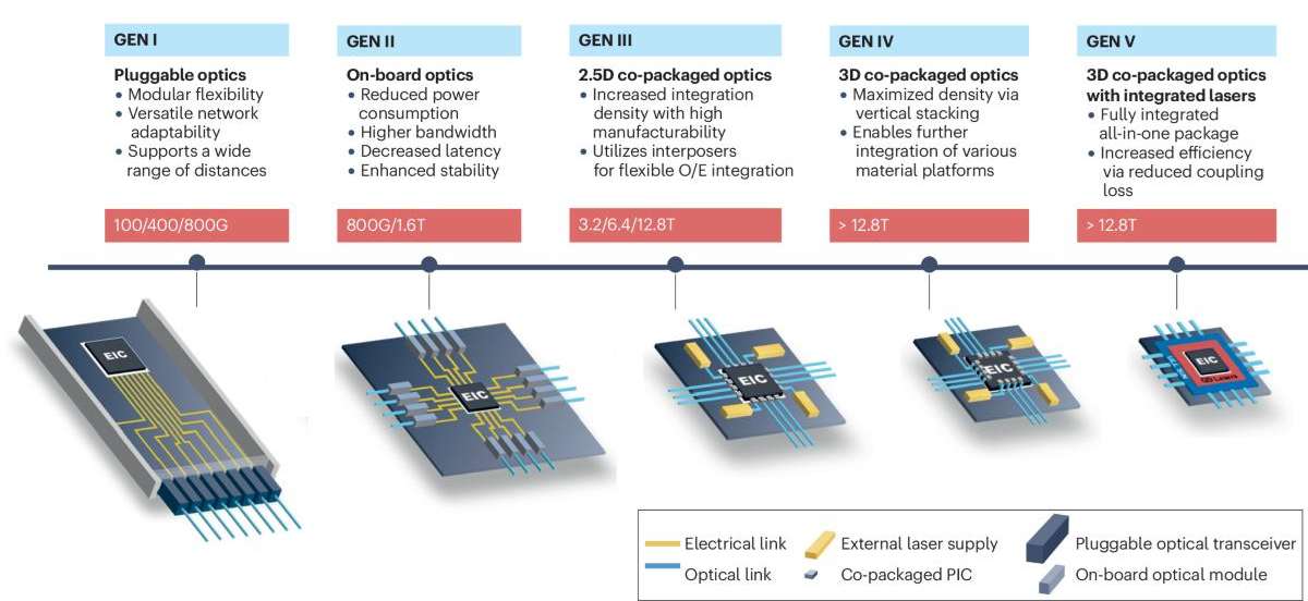
Figure 5. Packaging Evolution
• GEN I – Pluggable Optics
This generation uses external optical modules connected to systems through standard interfaces. It provides flexibility in deployment and easy replacement. Systems can adapt to different network requirements. However, electrical connections remain relatively long. This limits efficiency and increases power consumption.
• GEN II – On-Board Optics
Optical components are moved closer to the processing unit on the board. This reduces electrical trace length and improves signal integrity. It enables higher bandwidth and lower latency communication. Power consumption is reduced compared to pluggable solutions. System performance becomes more stable and efficient.
• GEN III – 2.5D Co-Packaged Optics
This stage introduces closer integration using interposer-based designs. Optical and electronic components are packaged together in a compact structure. It allows higher data density and improved signal routing. Bandwidth continues to scale significantly. This generation supports advanced data center requirements.
• GEN IV – 3D Co-Packaged Optics
Vertical stacking is introduced to maximize integration density. Multiple layers of components are combined within a single package. This enables shorter communication paths and higher efficiency. It supports integration of different material platforms. Performance improves significantly for high-speed systems.
• GEN V – Fully Integrated Photonics
This generation achieves full integration of optical and electronic components. Lasers and photonic elements are embedded within the package. It reduces coupling losses and improves efficiency. The system becomes highly compact and optimized. It represents the future direction of silicon photonics packaging.
Advantages of Silicon Photonics
• High data transmission speed for modern computing systems
• Supports extremely high bandwidth for large data workloads
• Lower power consumption compared to electrical interconnects
• Reduced signal loss over long distances
• Compact and scalable chip integration
• Compatible with existing CMOS manufacturing processes
• Enables faster communication in data centers and AI systems
Challenges of Silicon Photonics
• Difficult integration of efficient on-chip laser sources
• High manufacturing and packaging costs
• Thermal management issues due to heat sensitivity
• Complex alignment required for optical coupling
• Design complexity in large-scale integration
• Limited material compatibility for certain components
Applications of Silicon Photonics
1. Data Centers
Silicon photonics enables high-speed data transfer between servers and storage systems. It supports large-scale cloud computing infrastructure. Optical interconnects reduce latency and power consumption. This improves overall system efficiency.
2. Artificial Intelligence (AI) Systems
AI workloads require fast data movement between processors. Silicon photonics provides high bandwidth for parallel processing. It supports data handling in machine learning models. This enhances computational performance.
3. Telecommunications
It is used in fiber-optic communication networks for long-distance data transmission. Silicon photonics improves signal quality and bandwidth capacity. It supports high-speed internet and 5G infrastructure. This enables reliable global communication.
4. High-Performance Computing (HPC)
HPC systems benefit from faster interconnects between processors. Silicon photonics reduces communication bottlenecks. It supports large-scale simulations and scientific computing. This improves processing efficiency.
5. Sensing and Imaging
Silicon photonics is used in optical sensors for detecting environmental changes. It enables precise measurement of light signals. Applications include medical diagnostics and environmental monitoring. This improves accuracy and sensitivity.
6. Consumer Electronics
It is increasingly used in advanced devices requiring fast data transfer. Silicon photonics supports high-resolution displays and AR/VR systems. It enables compact and efficient designs. This enhances user experience.
Silicon Photonics vs Electrical Interconnect vs Fiber Optics
|
Feature |
Silicon
Photonics |
Electrical
Interconnect |
Fiber Optics |
|
Signal Type |
Optical
(on-chip, ~1310–1550 nm) |
Electrical
(copper traces) |
Optical (fiber,
~1310–1550 nm) |
|
Data Rate (per
lane) |
25–200 Gbps |
10–112 Gbps |
100–800+ Gbps |
|
Total Bandwidth |
>1 Tbps per
chip |
<1 Tbps
(limited by PCB) |
>10 Tbps (WDM
systems) |
|
Energy per Bit |
~1–5 pJ/bit |
~10–50 pJ/bit |
~5–20 pJ/bit |
|
Signal Loss |
~0.1–1 dB/cm
(on-chip) |
~5–20 dB/m
(high-speed PCB) |
~0.2 dB/km |
|
Transmission
Distance |
mm to ~2 km |
<1 m (high
speed) |
10 km to
>1000 km |
|
Integration
Level |
Chip-scale (CMOS
compatible) |
Board-level (PCB
traces) |
System-level
(fiber cables) |
|
Channel Density |
>100
channels/chip |
Limited by
routing space |
>100
channels/fiber (WDM) |
|
Latency |
~1–10 ps/mm |
~50–200 ps/cm |
~5 μs/km |
|
Heat Generation |
Low (minimal
resistive loss) |
High (I²R
losses) |
Very Low |
|
Footprint |
<10 mm²
(photonic IC) |
Large PCB area
required |
External fiber
links |
|
Design
Complexity |
High
(optical-electrical co-design) |
Low–Moderate |
Moderate |
|
Typical Use Case |
Chip-to-chip,
data centers, AI accelerators |
CPU, memory
buses, PCB links |
Long-haul
telecom, backbone networks |
|
Scalability
Limit |
Limited by
coupling & packaging |
Limited by
signal integrity |
Limited by
dispersion & amplification |
Conclusion
Silicon photonics sends data using light, which makes communication faster and more efficient than electrical signals. It works through key parts like waveguides, modulators, lasers, and photodetectors that handle the full signal process. Different designs and packaging methods help improve performance and make systems more compact. Even with some challenges, it is widely used in data centers, AI, telecom, and other high-speed applications.
About us
ALLELCO LIMITED
Read more
Quick inquiry
Please send an inquiry, we will respond immediately.
Frequently Asked Questions [FAQ]
1. What is the difference between silicon photonics and traditional optics?
Silicon photonics integrates optical components directly onto silicon chips, while traditional optics uses separate fiber-based systems. This allows smaller, faster, and more scalable designs.
2. How does silicon photonics improve data center performance?
It reduces latency, increases bandwidth, and lowers energy consumption, helping data centers handle massive data traffic more efficiently.
3. What materials are used in silicon photonics besides silicon?
Materials like germanium and III-V semiconductors are often used for photodetectors and lasers to improve performance and efficiency.
4. How does silicon photonics support 5G and future networks?
It enables high-speed, low-latency data transmission, which is critical for handling large-scale network traffic in 5G and beyond.
5. Is silicon photonics expensive to manufacture?
Yes, it can be costly due to complex fabrication and packaging processes, but costs are decreasing as technology matures.
USB-C vs USB PD: Complete Comparison Guide
on April 11th
EV Powertrain Explained: How It Works, Components, Types, and Applications
on April 10th
Popular Posts
-

Complex Instruction Set Computers: How They Changed Computing?
on April 17th 147721
-

USB-C Pinout and Features
on April 17th 111792
-

Using Xilinx Unified Simulation Primitives: A Comprehensive Guide to FPGA Design and Simulation
on April 17th 111328
-

Power Supply Voltages in Electronics: Meaning of VCC, VDD, VEE, VSS, and GND
on April 17th 83653
-

RJ45 Connector Guide: Pinout, Wiring, Cable Types, and Uses
on January 1th 79378
-

The Ultimate Guide to Wire Color Codes in Modern Electrical Systems
The way our electrical systems use colors isn’t just for looks. Each wire color now indicates a specific function, making it easier to identify and handle electrical components correctly during ins...on January 1th 66809
-

Quality (Q) Factor: Equations and Applications
The quality factor, or 'Q', is important when checking how well inductors and resonators work in electronic systems that use radio frequencies (RF). 'Q' measures how well a circuit minimizes energy...on January 1th 62968
-

Purge Valve Guide: Function, Symptoms, Testing, and Replacement for Optimal Engine Performance
The purge valve is a key part of a car’s system that helps keep the air clean by managing fuel vapors before they can escape into the atmosphere. This not only helps the environment by reducing pol...on January 1th 62865
-

Achieving Peak Performance with the Maximum Power Transfer Theorem
The Maximum Power Transfer Theorem explains how energy from a source, such as a battery or generator, flows to a connected load. It shows the exact condition where the load receives the most power....on January 1th 54050
-

A23 Battery Specifications and Compatibility
The A23 battery is a small, cylinder-shaped battery with high voltage. Also called 23A, 23AE, or MN21, it runs at 12 volts and much higher than AA or AAA batteries. Its special design make...on January 1th 52032
HOT Part Number
-

CC0805KRX7RABB102
YAGEO
CAP CER 1000PF 200V X7R 0805
MCH6448-TL-H
onsemi
MOSFET N-CH 20V 8A 6MCPH
MP6302DD-LF-Z
Monolithic Power Systems Inc.
IC ENERGY STORAGE QFN10
GRM0335C1H100FA01D
Murata Electronics
CAP CER 10PF 50V C0G/NP0 0201
SN65LVELT22DGKR
Texas Instruments
IC TRANSLATOR UNIDIR 8VSSOP
5M80ZM68I5N
Intel
IC CPLD 64MC 7.5NS 68MBGA
TPS3824-50DBVRG4
Texas Instruments
IC 5.0V SUPPLY MONITOR SOT-23-5
PIC12C672-04I/SM
Microchip Technology
IC MCU 8BIT 3.5KB OTP 8SOIJ
08055C243JAT4A
KYOCERA AVX
CAP CER 0.024UF 50V X7R 0805
MT25QL256ABA8ESF-0AAT
Micron Technology Inc.
IC FLASH 256MBIT SPI 16SOP2
NCP57152MNADJTYG
onsemi
IC REG LINEAR POS ADJ 1.5A 8DFN
FW82801CA
Intel
82801 - I/O CONTROLLER HUB
SN74AS580N
Texas Instruments
BUS DRIVER, AS SERIES
SNJ54HC163J
Texas Instruments
54HC163 SYNCHRONOUS 4-BIT BINARY
UPD78F0441GB-GAH-AX
Renesas Electronics America Inc
IC MCU 8BIT 16KB FLASH 64LQFP
GRM1556T1H7R3CD01D
Murata Electronics
CAP CER 7.3PF 50V T2H 0402
HUF75307D3
Harris Corporation
MOSFET N-CH 55V 15A IPAK
TMP431DDGKR
Texas Instruments
SENSOR DIGITAL -40C-125C 8VSSOP -

NTMS3P03R2G
onsemi
MOSFET P-CH 30V 2.34A 8SOIC
04025C221KAT2A
KYOCERA AVX
CAP CER 220PF 50V X7R 0402
74439344047
Würth Elektronik
WE-XHMI SMT POWER INDUCTOR 4.7 U
MA2J11400L
Panasonic Electronic Components
DIODE GP 150V 200MA SMINI2-F1
ISL8491IBZ
Renesas Electronics America Inc
IC TRANSCEIVER FULL 1/1 14SOIC
A3P250L-FGG144
Microsemi Corporation
IC FPGA 97 I/O 144FBGA
TLV73318PQDRVRQ1
Texas Instruments
IC REG LINEAR 1.8V 300MA 6WSON
SN74ABT18640DLR
Texas Instruments
IC SCAN TEST DEVICE 18BIT 56SSOP
LM3S611-IGZ50-C2
Texas Instruments
IC MCU 32BIT 32KB FLASH 48VQFN
EMK316BJ225KLHT
Taiyo Yuden
CAP CER 2.2UF 16V X5R 1206
1N2232A
Microchip Technology
DIODE GEN PURP 300V 5A DO4
1PMT33AT1
onsemi
TVS DIODE 33VWM 53.3VC POWERMITE
STN1NK60Z
STMicroelectronics
MOSFET N-CH 600V 300MA SOT223
MIC5238-1.1YD5
Microchip Technology
IC REG LIN 1.1V 150MA TSOT23-5
SA5.0A
Taiwan Semiconductor Corporation
TVS DIODE 5VWM 9.2VC DO204AC
1SMA4740_R1_00001
Panjit International Inc.
SURFACE MOUNT SILICON ZENER DIOD
08055C682KAJ2A
KYOCERA AVX
CAP CER 6800PF 50V X7R 0805
XC7A12T-L2CSG325E
AMD
IC FPGA 150 I/O 324CSBGA -

STMP3770XXBJEA2N
NXP USA Inc.
STMP3770XXBJEA2N
RJK1028DNS-00#J5
Renesas Electronics America Inc
ABU / MOSFET
MC14490DWG
onsemi
IC ELIMINATOR BOUNCE HEX 16SOIC
LTC4373HDD#PBF
Analog Devices Inc.
LOW ICC IDEAL DIODE CONTROLLER W
ADS131A04IPBSR
Texas Instruments
IC AFE 4 CHAN 24BIT 32TQFP
FH23-39S-0.3SHW(10)
Hirose Electric Co Ltd
CONN FPC BOTTOM 39POS 0.3MM R/A
XL1010-QT-0G0T
MACOM Technology Solutions
IC RF AMP GPS 20GHZ-38GHZ 16QFN
CYBL10461-56LQXIT
Infineon Technologies
IC RF TXRX+MCU BLUETOOTH 56UFQFN
AM26LS31CDB
Texas Instruments
IC QUAD DIFF LINE RCVR 16SSOP
AM26LV31CD
Texas Instruments
IC DRIVER 4/0 16SOIC
SN74AUC1G74RSER
Texas Instruments
IC FF D-TYPE SNGL 1BIT 8UQFN
BZG03C240TR3
Vishay General Semiconductor - Diodes Division
DIODE ZENER 240V 1.25W DO214AC
74VCXH16245DTRG
onsemi
IC TXRX NON-INVERT 3.6V 48TSSOP
UPSD3434E-40U6
STMicroelectronics
IC MCU 8BIT 288KB FLASH 80LQFP
JM38510/02306BCA
Texas Instruments
NAND GATE
APX803L05-35SA-7
Diodes Incorporated
IC SUPERVISOR 1 CHANNEL SOT23
ATS030A0X3-SRZ
ABB Power Electronics Inc.
DC DC CONVERTER 0.8-2.75V 80W
VI-262-CX
Vicor Corporation
DC DC CONVERTER 15V 75W