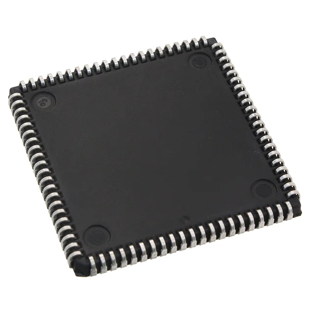
XC3042-100PC84C PLCC84 Package, Logic Blocks, and Performance
The XC3042-100PC84C is a classic programmable logic device from the well-known XC3000 family. It gives you a flexible way to handle digital logic without relying on fixed-function chips. With around 3000 usable gates and 5V operation, it fits perfectly into older boards and long-running systems. You can reprogram it by loading configuration data at power-up, which makes updates much easier. Its 84-pin PLCC package keeps board layouts compact while still offering plenty of I/O connections. From industrial machines to retro computing projects, this device continues to support reliable hardware designs. Here, you’ll get a clear look at its features, structure, and real-world uses.Catalog
XC3042-100PC84C Overview
The XC3042-100PC84C is a CMOS SRAM based field programmable gate array designed for configurable digital logic implementation. It belongs to the XC3000 family and is supplied in an 84 pin PLCC package. The device operates with a 5 volt supply and requires configuration data at power up to define its logic functions. Its internal structure supports programmable logic blocks and flexible input and output connections for control, interface, and data handling tasks. This component is commonly used in embedded systems, industrial equipment, and legacy digital platforms that require adaptable hardware logic. Looking for XC3042-100PC84C Contact us to check current stock, lead time, and pricing.
Typical Icc vs. Frequency for XC3042-100PC84C
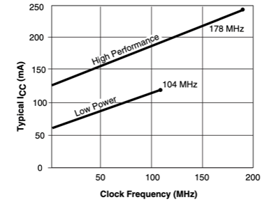
Graph plots typical supply current on the vertical axis in milliamps against clock frequency on the horizontal axis in megahertz, showing current increasing with operating frequency. Two operating modes are identified, labeled Low Power and High Performance, each represented by a rising line. Low Power mode reaches approximately 104 MHz at a current near 120 mA, while High Performance mode extends to about 178 MHz with current approaching 240 mA. The linear trend in both curves indicates proportional growth of dynamic current consumption as switching frequency increases, reflecting frequency dependent power characteristics of the device.
XC3042-100PC84C CAD Model
XC3042-100PC84C Symbol

XC3042-100PC84C Footprint

XC3042-100PC84C 3D Model
Features of XC3042-100PC84C
Usable Logic Gate Capacity
XC3042-100PC84C provides approximately 3000 usable logic gates for implementing digital circuits. This capacity supports control logic, data routing, state machines, and arithmetic operations within a single programmable device. By integrating multiple logic functions into one component, it reduces the need for separate fixed logic ICs and supports compact board layouts.
Configurable Logic Block Structure
The device contains 144 Configurable Logic Blocks that form the core of its programmable architecture. Each block can be arranged to perform combinational and sequential logic functions. This structure allows designers to define custom hardware behavior based on application requirements while maintaining predictable digital operation.
User Input And Output Resources
XC3042-100PC84C includes 74 user accessible input and output pins. These pins enable direct connection to external memory, processors, control lines, and communication interfaces. The available I O count supports flexible system integration in embedded and legacy platforms.
Integrated On Chip Memory
The device incorporates 30784 total RAM bits within its internal structure. This memory can be used for temporary data storage, buffering, and logic related functions. Having built in RAM reduces reliance on external memory for moderate storage needs.
Standard 5 Volt Operating Range
XC3042-100PC84C operates within a supply voltage range of 4.75 volts to 5.25 volts. This range aligns with standard 5 volt digital systems and supports compatibility with TTL and CMOS based circuits commonly used in established designs.
Commercial Temperature Range
The specified operating temperature range is 0 degrees Celsius to 85 degrees Celsius. This makes the device suitable for controlled indoor commercial and industrial environments where stable thermal conditions are maintained.
84 Pin PLCC Package Format
The device is supplied in an 84 pin Plastic Leaded Chip Carrier package with J leads. This surface mount format supports secure board attachment and efficient use of printed circuit board space in medium density layouts.
SRAM Based Reprogrammable Architecture
XC3042-100PC84C uses an SRAM based configuration system. Its logic configuration is loaded at power up from an external source, allowing the device to be reprogrammed when design updates are required. This supports design flexibility without hardware replacement.
XC3000 Family Architecture Compatibility
The device follows the architecture of the XC3000 FPGA family. It supports established configuration methods and design approaches used within this product series, enabling consistent integration with related devices.
Speed Grade -100 Timing Classification
The -100 speed grade defines the timing performance category of the device. It indicates switching and propagation characteristics within the XC3000 family, supporting stable and predictable digital signal behavior in practical applications.
XC3042-100PC84C Technical Specifications
| Product Attribute | Attribute Value |
| Manufacturer | AMD Xilinx |
| Voltage - Supply | 4.75V ~ 5.25V |
| Total RAM Bits | 30784 |
| Supplier Device Package | 84-PLCC (29.31x29.31) |
| Series | XC3000 |
| Package / Case | 84-LCC (J-Lead) |
| Package | Tray |
| Operating Temperature | 0°C ~ 85°C (TJ) |
| Number of LABs/CLBs | 144 |
| Number of I/O | 74 |
| Number of Gates | 3000 |
| Mounting Type | Surface Mount |
| Base Product Number | XC3042 |
| RoHs Status | RoHS non-compliant |
| Moisture Sensitivity Level (MSL) | 3 (168 Hours) |
| REACH Status | REACH Unaffected |
| ECCN | EAR99 |
| HTSUS | 8542.39.0001 |
Architecture of XC3042-100PC84C
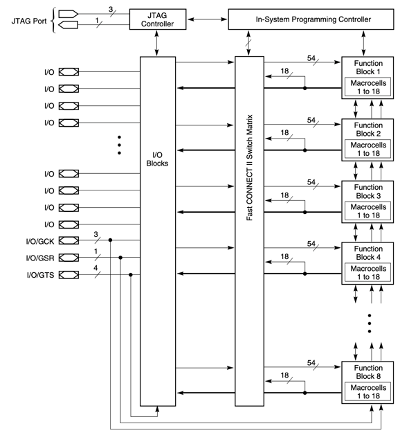
Structured around eight function blocks, each containing 18 macrocells, the device connects programmable logic resources through a central FastCONNECT II switch matrix that manages internal signal routing. Each function block interfaces with the matrix using 54 input lines and 18 output paths, supporting predictable interconnect delays typical of CPLD structures. I/O blocks positioned along the left side provide external pin connectivity and integrate global control signals labeled I O GCK, I O GSR, and I O GTS for clock, set reset, and tristate distribution. A JTAG controller and in system programming controller appear at the top, indicating boundary scan compliance and reprogrammable configuration capability. Bold signal paths show direct connections from function block outputs to the I O blocks, reducing routing stages for selected outputs.
AC Load Circuit of XC95144XL
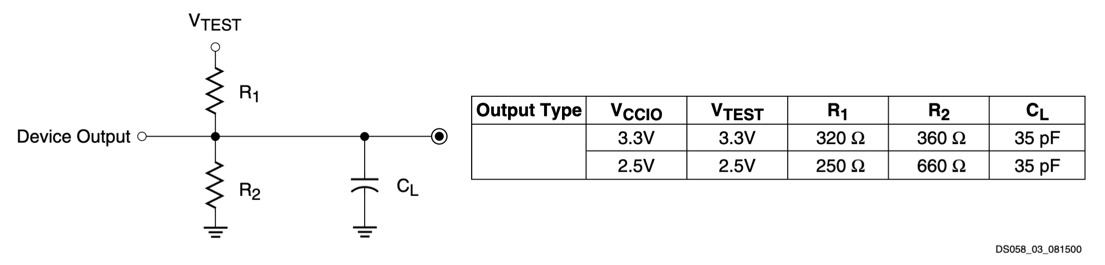
Test load configuration connects the device output to a resistive divider formed by R1 tied to VTEST and R2 tied to ground, with a capacitive load CL connected from the output node to ground. The circuit models output switching conditions for AC timing measurements by defining controlled resistive and capacitive loading. A table specifies values for two operating levels, with VCCIO and VTEST set to 3.3 V using R1 of 320 ohms and R2 of 360 ohms, or 2.5 V using R1 of 250 ohms and R2 of 660 ohms, while CL remains 35 pF in both cases. This configuration establishes standardized loading parameters to evaluate output rise and fall characteristics under defined voltage conditions.
Applications of XC3042-100PC84C
Legacy Embedded System Maintenance
The XC3042-100PC84C is widely used to maintain embedded systems developed during the early adoption of programmable logic. Many control boards in manufacturing equipment, instrumentation, and communication hardware were designed around the XC3000 architecture. When these systems require repair, the device allows the original programmable logic to be restored without modifying the printed circuit board. This helps preserve system behavior, timing relationships, and signal compatibility.
Industrial Control Systems Based on XC3000 Architecture
In industrial control platforms built with XC3000 series devices, the XC3042-100PC84C manages sequencing, signal routing, and interface coordination between sensors and actuators. Its 5 volt operating range matches the logic levels used in older automation systems. The device can handle timing control, data path management, and discrete logic replacement within programmable hardware, allowing stable operation in long running production environments.
Retro Computing And Hardware Restoration Projects
The XC3042-100PC84C is used in retro computing projects that aim to preserve or recreate early programmable logic designs. It enables restoration of expansion cards, development boards, and interface modules originally built with XC3042 devices. By supporting the same configuration structure and pin layout, it helps maintain authentic hardware behavior while allowing reprogramming when design files are available.
Educational Study Of Early FPGA Architecture
The device serves as a teaching platform for understanding first generation SRAM based FPGA structures. Students can examine configurable logic blocks, internal memory resources, and external configuration methods in a real hardware device. Working with this architecture provides practical insight into how early programmable logic systems were organized and how digital functions were mapped into hardware.
Direct Replacement In Existing XC3042 Installations
The XC3042-100PC84C functions as a drop in replacement for systems that already use XC3042 series components. It supports the same package format, voltage range, and architectural structure, allowing repair or refurbishment of aging equipment. This approach extends the service life of legacy systems without requiring redesign or conversion to newer programmable platforms.
Device Part Marking XC3042-100PC84C
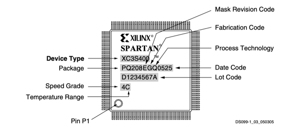
Package illustration presents the top view of a TQ144 device with labeled part marking fields that define ordering information. Device type appears as XC95xxxXL, indicating the family designation, while the package code TQ144 identifies the 144 pin thin quad flat package. Speed grade is marked as 7C, where the numeric value denotes timing performance and the letter indicates the commercial operating temperature range. A separate horizontal line is shown as not related to the device part number, distinguishing traceability or lot information from ordering identifiers. Pin 1 location is marked by a circular indicator at one corner to define package orientation.
XC3042-100PC84C Advantages and Disadvantages
Advantages
• SRAM based structure allows logic to be reprogrammed when design changes are required
• Established XC3000 architecture supports stable operation in long term legacy systems
• 5 volt supply range matches older TTL and CMOS logic levels
• Moderate gate count fits small to medium scale digital control tasks
• Commonly integrated in earlier embedded and industrial platforms
• 84 pin PLCC package supports compact surface mount board layouts
Disadvantages
• 5 volt operation does not align with modern low voltage digital systems
• Logic capacity is limited compared to current generation FPGA devices
• Power consumption is higher than newer low voltage programmable logic families
• Lacks embedded multipliers and dedicated signal processing resources
• Does not include advanced clock management or high speed interface features
• Development tool compatibility is restricted in modern FPGA design environments
XC3042-100PC84C Alternatives
| Part Number | Manufacturer | Key Features | Use Case/Notes |
| XC3042-100PQ100C | AMD | XC3000 family FPGA with around 3,000 system gates and 144 configurable logic blocks. Operates from a 5V supply and supports surface-mount packaging. | Used in legacy programmable logic designs, interface control, and moderate-density digital applications. |
| XC3042-125PQ100C | AMD | Similar XC3042 device with alternate speed grade. Provides configurable logic resources and flexible I/O in a PQFP package. | Appropriate for digital control and communication circuits where timing requirements are moderate. |
| XC3030L-8VQ64C | AMD | Low-power FPGA from the XC3000L series with configurable logic blocks and compact package design. Designed for reduced power consumption. | Suitable for power-sensitive embedded systems and consumer electronic products. |
| XC3030L-8VQ64I | AMD | Industrial-grade low-power FPGA with extended temperature range and flexible programmable logic resources. | Used in industrial control and embedded systems requiring reliable operation in harsher environments. |
About AMD Xilinx
AMD Xilinx operates as the adaptive and embedded computing division of Advanced Micro Devices, Inc. The organization traces its origins to Xilinx, Inc., founded in 1984 in California, where it introduced programmable logic devices that could be configured after manufacturing. Over the years, the company expanded into programmable platforms used in communications infrastructure, industrial automation, aerospace systems, automotive electronics, and data center acceleration. Its portfolio includes programmable logic devices, adaptive system on chip platforms, development software, and design tools that support hardware level customization. Following its acquisition by AMD in 2022, its technologies became part of a broader semiconductor portfolio that combines programmable logic with high performance processing solutions.
Conclusion
The XC3042-100PC84C gives you a practical way to manage programmable logic in 5V digital systems. With its SRAM-based structure, you can reload and update the configuration whenever needed. It offers a solid mix of logic capacity, internal RAM, and flexible I/O connections. The PLCC84 package keeps it easy to integrate into many board layouts. Whether you are maintaining older equipment or working on restoration projects, this device helps you keep original hardware running smoothly. It remains a dependable choice when compatibility and flexibility matter.
Datasheet PDF
XC3042-100PC84C Datasheet:
About us
ALLELCO LIMITED
Read more
Quick inquiry
Please send an inquiry, we will respond immediately.
Frequently Asked Questions [FAQ]
1. What type of device is the XC3042-100PC84C?
The XC3042-100PC84C is a CMOS SRAM-based field programmable gate array (FPGA). It belongs to the XC3000 family and allows you to define custom digital logic by loading configuration data at power-up. This means you can change how it works without replacing the hardware.
2. What supply voltage does the XC3042-100PC84C require?
It operates within a 4.75V to 5.25V range, which matches standard 5V digital systems. This makes it compatible with many older TTL and CMOS circuits commonly found in legacy boards.
3. How many logic resources does the XC3042-100PC84C provide?
The device offers about 3000 usable logic gates and includes 144 configurable logic blocks. It also features 74 user-accessible I/O pins and over 30,000 bits of internal RAM for temporary data storage and logic functions.
4. Can the XC3042-100PC84C be reprogrammed after installation?
Yes, it can. Since it uses SRAM-based configuration, you can load new configuration data each time the system powers up. This allows updates and design changes without physically replacing the chip.
5. Where is the XC3042-100PC84C commonly used?
You’ll often find it in embedded systems, industrial control equipment, and retro computing projects. It is especially useful when maintaining or restoring hardware built around the XC3000 architecture.
Understanding MPC8548EVUAUJ Block Diagram and Performance Capabilities
on February 18th
4.7 kΩ Resistor Guide: Color Code, Uses, Testing & Value Comparison
on February 16th
Popular Posts
-

Complex Instruction Set Computers: How They Changed Computing?
on April 18th 147758
-

USB-C Pinout and Features
on April 18th 111954
-

Using Xilinx Unified Simulation Primitives: A Comprehensive Guide to FPGA Design and Simulation
on April 18th 111349
-

Power Supply Voltages in Electronics: Meaning of VCC, VDD, VEE, VSS, and GND
on April 18th 83722
-

RJ45 Connector Guide: Pinout, Wiring, Cable Types, and Uses
on January 1th 79508
-

The Ultimate Guide to Wire Color Codes in Modern Electrical Systems
The way our electrical systems use colors isn’t just for looks. Each wire color now indicates a specific function, making it easier to identify and handle electrical components correctly during ins...on January 1th 66921
-

Purge Valve Guide: Function, Symptoms, Testing, and Replacement for Optimal Engine Performance
The purge valve is a key part of a car’s system that helps keep the air clean by managing fuel vapors before they can escape into the atmosphere. This not only helps the environment by reducing pol...on January 1th 63078
-

Quality (Q) Factor: Equations and Applications
The quality factor, or 'Q', is important when checking how well inductors and resonators work in electronic systems that use radio frequencies (RF). 'Q' measures how well a circuit minimizes energy...on January 1th 63017
-

Achieving Peak Performance with the Maximum Power Transfer Theorem
The Maximum Power Transfer Theorem explains how energy from a source, such as a battery or generator, flows to a connected load. It shows the exact condition where the load receives the most power....on January 1th 54082
-

A23 Battery Specifications and Compatibility
The A23 battery is a small, cylinder-shaped battery with high voltage. Also called 23A, 23AE, or MN21, it runs at 12 volts and much higher than AA or AAA batteries. Its special design make...on January 1th 52147
HOT Part Number
-

MMSZ4684
onsemi
DIODE ZENER 3.3V 500MW SOD123
74ACT74SC
onsemi
IC FF D-TYPE DUAL 1BIT 14SOIC
SN65EPT23D
Texas Instruments
IC TRANSLTR UNIDIRECTIONAL 8SOIC
1N3211R
GeneSiC Semiconductor
DIODE GEN PURP REV 300V 15A DO5
CYRF89235-40LTXC
Infineon Technologies
IC RF TXRX+MCU ISM>1GHZ 40VFQFN
LTM4606MPV#PBF
Analog Devices Inc.
DC DC CONVERTER 0.6-5V
AP3585AMPTR-G1
Diodes Incorporated
IC REG CTRLR BUCK 8SO
G3VM-S1
Omron Electronics Inc-EMC Div
SSR RELAY SPST-NO 400MA 0-60V
XC6219B332MR
UMW
300MA 40DB@(1KHZ) 280MV@(100MA)
MAX749CSA+
Analog Devices Inc./Maxim Integrated
IC LCD BIAS SUPPLY DGT ADJ 8SOIC
PI7C8150BNDE
Diodes Incorporated
IC INTERFACE SPECIALIZED 256BGA
TLZ6V2B-GS08
Vishay General Semiconductor - Diodes Division
DIODE ZENER 6.2V 500MW SOD80
MA302GQ-P
Monolithic Power Systems Inc.
SENSOR ANGLE SMD
LTC1841CS8#TRPBF
Analog Devices Inc.
IC COMPARATOR 2 GEN PUR 8SO
AXK650337YG
Panasonic Electric Works
CONN HDR 50POS SMD GOLD
SL44-M3/57T
Vishay General Semiconductor - Diodes Division
DIODE SCHOTTKY 40V 4A DO214AB
NB600CQ-LF-Z
Monolithic Power Systems Inc.
IC REG BUCK SYNC 3.6V 3A
A1120EUA-T
Allegro MicroSystems
MAGNETIC SWITCH UNIPOLAR 3SIP -

N74F04D,623
Nexperia USA Inc.
IC INVERTER 6CH 1-INP 14SO
SMBJ54A
SMC Diode Solutions
TVS DIODE 54VWM 87.1VC SMB
STK672-442BN-E
onsemi
IC MOTOR DRIVER UNIPOLAR 19SIP
BA178M20FP-E2
Rohm Semiconductor
IC REG LINEAR 20V 500MA TO252-3
FL77904MX
onsemi
IC LED DRV OFFL TRIAC 8SOP
XC7S25-1CSGA225C
AMD
IC FPGA 150 I/O 225CSGA
T491C226K010AS
KEMET
CAP TANT 22UF 10% 10V 2312
LT3020EMS8-1.2#PBF
Analog Devices Inc.
IC REG LINEAR 1.2V 100MA 8MSOP
AT25DF021A-MAHN-T
Adesto Technologies
IC FLASH 2MBIT SPI 104MHZ 8UDFN
LT5526EUF#PBF
Analog Devices Inc.
IC MIXR 1KHZ-2GHZ DWN CONV 16QFN
AT28BV64-25TC
Microchip Technology
IC EEPROM 64KBIT PARALLEL 28TSOP
SMP100LC-35
STMicroelectronics
THYRISTOR 35V 400A DO214AA
SI7457DP-T1-GE3
Vishay Siliconix
MOSFET P-CH 100V 28A PPAK SO-8
S25FL132K0XMFV011
Infineon Technologies
IC FLASH 32MBIT SPI/QUAD 8SOIC
C3216X5R1A107M160AC
TDK Corporation
CAP CER 100UF 10V X5R 1206
AON6362FD
Alpha & Omega Semiconductor Inc.
MOSFET N-CH 30V 27A/60A 8DFN
SRP7050TA-100M
Bourns Inc.
FIXED IND 10UH 4A 69 MOHM SMD
AQW454
Panasonic Electric Works
SSR RELAY SPST-NC 120MA 0-400V -

AM26LV32CDR
Texas Instruments
IC RECEIVER 0/4 16SOIC
ACS724LLCTR-05AB-T
Allegro MicroSystems
SENSOR CURRENT HALL
SN74CBT3384ADBQR
Texas Instruments
IC BUS SWITCH 5 X 1:1 24SSOP
HUF76429D3
Fairchild Semiconductor
N-CHANNEL POWER MOSFET
MAX4224EUT+T
Analog Devices Inc./Maxim Integrated
IC OPAMP CFA 1 CIRCUIT SOT6
CSD23285F5T
Texas Instruments
MOSFET P-CH 12V 5.4A 3PICOSTAR
ISL6627CRZ-T
Renesas Electronics America Inc
IC REG CTRLR INTEL 1OUT 10DFN
REF195GSZ-REEL7
Analog Devices Inc.
IC VREF SERIES 0.2% 8SOIC
LT1076CR-5#PBF
Analog Devices Inc.
IC REG MULTI CONFG 5V 2A D2PAK-7
MIC5308-1.2YD6
Micrel Inc.
IC REG LINEAR LO VIN/VOUT 150MA
AD2S80AKD
Analog Devices Inc.
IC R/D CONV 10/12/14/16B 40CDIP
74HC541D,653
Nexperia USA Inc.
IC BUFFER NON-INVERT 6V 20SO
TP3069N
Texas Instruments
IC CODEC FILTER CMOS 20DIP
GRM155R70G105KA12D
Murata Electronics
CAP CER 1UF 4V X7R 0402
1808SC152KAT1A
KYOCERA AVX
CAP CER 1500PF 1.5KV X7R 1808
ADT75BRMZ-REEL7
Analog Devices Inc.
SENSOR DIGITAL -55C-125C 8MSOP
PPD6-48-1515
TDK-Lambda Americas Inc
DC DC CONVERTER +/-15V 6W
SN74ALS244CDWR
Texas Instruments
IC BUF NON-INVERT 5.5V 20SOIC