XC4085XLA-08BG432C FPGA Specifications and Design Overview
You get a clear look at what the XC4085XLA-08BG432C offers when flexible hardware logic is part of your system. This device lets you shape digital behavior through configuration, then adjust it later without touching the board. With a solid balance of logic capacity and a high number of connections, it fits designs that handle many signals at once. You can rely on stable timing, steady power distribution, and predictable operation over long runtimes. That makes it a comfortable choice for control, communication, and embedded platforms that may change over time.Catalog
XC4085XLA-08BG432C Overview
The XC4085XLA-08BG432C is a reprogrammable logic device designed for digital systems that need flexible hardware control. It allows designers to define and update logic functions after deployment, supporting changes without altering physical circuitry. The device offers moderate logic capacity with a large number of input and output connections, making it suitable for systems that interface with multiple signals. Its architecture supports stable timing behavior and consistent operation across extended runtimes. Typical uses include industrial control units, communication equipment, and embedded processing boards where adaptable logic and long service life are required.
Looking for XC4085XLA-08BG432C? Contact us to check current stock, lead time, and pricing.
Power Distribution of XC4085XLA-08BG432C
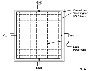
Power distribution is arranged using a perimeter ring and an internal grid to supply stable voltage across the device. Dedicated Vcc and GND connections are positioned at the midpoints of each side, feeding a continuous power ring that surrounds the core logic and supports the I O driver circuits. Inside the ring, a uniform logic power grid spans the full array to distribute operating voltage evenly to all logic blocks. This structure minimizes voltage variation across the die and supports consistent operation by separating core logic power from input and output driver supply paths while maintaining a symmetrical layout.
Features of XC4085XLA-08BG432C
Logic Block Organization and Capacity
The device includes 3136 logic array blocks that form the foundation for building custom digital functions. These blocks can be configured to handle control logic, data handling, and coordination tasks within a single programmable structure. This organization supports flexible design changes without altering the physical layout of the system.
System Gate Count for Integrated Logic Functions
With an estimated capacity of about 55,000 system gates, the XC4085XLA-08BG432C can support multiple logic functions operating together. This allows designers to consolidate tasks that would otherwise require several fixed logic components, helping simplify overall system design.
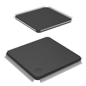
High Density Ball Grid Array Package
The 432 ball grid array package provides a large number of external connections in a compact 40 × 40 form factor. This layout supports complex signal routing while conserving board space, making it suitable for designs with extensive input and output requirements.
Commercial Temperature Operating Range
The device operates within a junction temperature range of 0°C to 85°C. This range supports stable performance in controlled environments where consistent electrical behavior is required during continuous operation.
Reconfigurable Logic for Embedded System Use
The internal logic can be reprogrammed to adjust system behavior after deployment. This capability supports updates, refinements, and functional changes over time, making the device suitable for embedded systems with evolving design needs.
XC4085XLA-08BG432C Technical Specifications
| Product Attribute | Attribute Value |
| Manufacturer | AMD Xilinx |
| Supplier Device Package | 432-MBGA (40x40) |
| Series | XC4000XLA/XV |
| Package / Case | 432-LBGA Exposed Pad, Metal |
| Package | Bulk |
| Operating Temperature | 0°C ~ 85°C (TJ) |
| Number of LABs / CLBs | 3136 |
| Number of Gates | 55000 |
| Mounting Type | Surface Mount |
| RoHS Status | RoHS non-compliant |
| Moisture Sensitivity Level (MSL) | 3 (168 Hours) |
| REACH Status | REACH Affected |
| ECCN | 3A991D |
| HTSUS | 8542.39.0001 |
Simplified Block Diagram of XC4085XLA-08BG432C
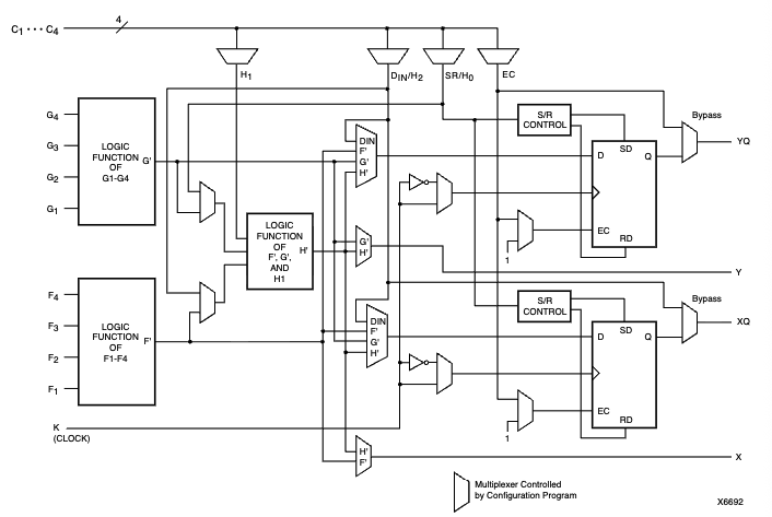
Internal structure is organized around a configurable logic block containing two primary logic sections labeled F and G, each driven by four inputs and implemented using programmable logic functions. Outputs from these sections can be combined through an additional logic path labeled H to support wider logic operations. Multiple configuration controlled multiplexers manage signal selection between direct inputs, feedback paths, and combined logic results. Two independent storage elements are included, each supporting clocked operation with enable and set reset control, while bypass paths allow unregistered signals to reach routing outputs. Shared control signals such as clock, enable, and reset distribute across the block to support synchronous operation, and labeled outputs provide both registered and combinational signal paths for flexible internal routing within the device.
Fast Carry Logic in XC4085XLA-08BG432C
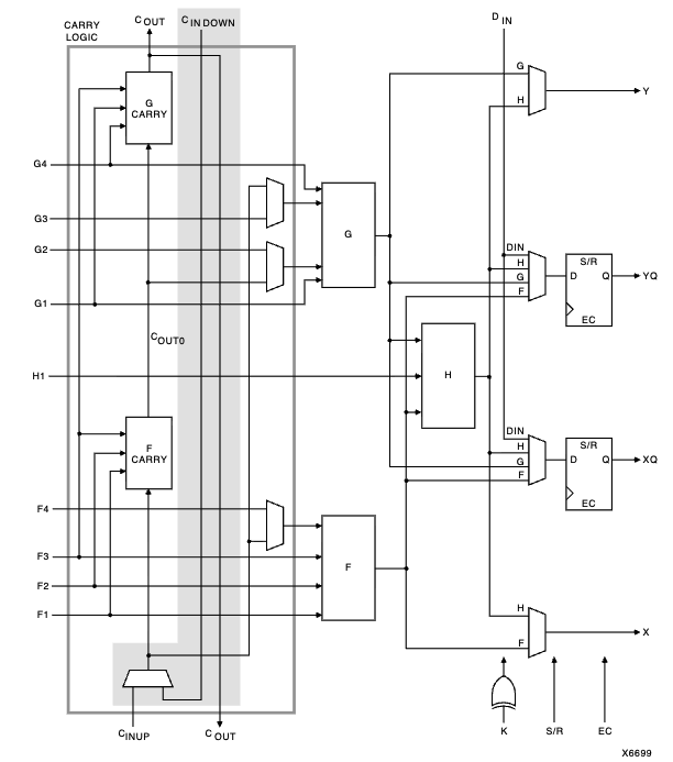
Carry path structure is integrated alongside the standard logic functions to support arithmetic operations with reduced propagation delay. Separate F and G logic sections receive four inputs each and connect directly to dedicated carry blocks labeled F CARRY and G CARRY, enabling fast carry generation and propagation. Vertical carry chains link adjacent blocks through CIN and COUT signals, allowing addition and comparison functions to extend efficiently across multiple logic blocks. The shaded region indicates the enhanced carry circuitry present in XC4000E devices, which is not included in XC4000X variants. Outputs from the logic and carry paths are routed through configurable multiplexers and optional storage elements with shared clock, enable, and set reset controls, providing both registered and unregistered result paths within the device.
Applications of XC4085XLA-08BG432C
Industrial Automation and Control Systems
The XC4085XLA-08BG432C is used in industrial automation systems to handle programmable control logic and coordination tasks. It supports signal processing, timing control, and system sequencing in equipment such as controllers and monitoring units. Its reconfigurable structure allows logic behavior to be adjusted as process requirements change, without redesigning the hardware.
Telecommunications and Networking Equipment
In telecommunications and networking equipment, the device supports control logic, interface handling, and data flow management. It is applied in systems where protocols or operating modes may evolve over time. The ability to update logic through configuration helps extend system usability while maintaining consistent operation.
Medical Electronics with Moderate Logic Complexity
The device is suitable for medical electronic systems that rely on stable digital control and structured data handling. It can be used in diagnostic devices, monitoring equipment, and control subsystems operating in regulated environments. Its predictable behavior supports designs where reliability and repeatable performance are required.
Aerospace and Defense Subsystems in Controlled Environments
The XC4085XLA-08BG432C is applied in aerospace and defense subsystems that operate within defined temperature limits. It supports custom logic for control, monitoring, and data coordination tasks. The reprogrammable nature allows updates during long system lifecycles without physical modification.
Embedded Control and Data Processing Platforms
In embedded platforms, the device supports control logic combined with basic data processing functions. It is used to connect processors, memory, and peripherals through adaptable logic structures. This flexibility makes it suitable for embedded systems that must adapt to changing functional requirements over time.
XC4085XLA-08BG432C Advantages and Disadvantages
Advantages
• Reconfigurable logic allows functional updates after system deployment
• Logic capacity supports mid scale control and embedded digital designs
• Architecture offers stable behavior with well defined operating characteristics
• BGA package enables high input and output integration in compact layouts
Disadvantages
• RoHS non compliant status limits use in restricted environmental designs
• Moisture sensitivity level requires controlled storage and handling
• Temperature range is narrower than extended or industrial grade options
• Architecture reflects an earlier generation of programmable logic devices
XC4085XLA-08BG432C Alternatives
| Part Number | Manufacturer | Key Features | Use Case/Notes |
| XC4085XLA-09BG352I | AMD | Low-power FPGA from the XC4000XLA family with solid logic capacity and support for industrial temperature operation. | Used in industrial control, embedded systems, and applications requiring stable performance over a wide temperature range. |
| XC4085XL-3BG432C | AMD | FPGA from the XC4000XL series optimized for commercial temperature ranges and surface-mount integration. | Suitable for commercial electronics, digital control boards, and general-purpose FPGA-based designs. |
| XC4085XL-3BG432I | AMD | Industrial-temperature variant of the XC4000XL FPGA, maintaining the same logic features with enhanced environmental tolerance. | Ideal for industrial automation, communication equipment, and systems exposed to harsher operating conditions. |
About AMD Xilinx
AMD Xilinx is a technology company known for developing programmable logic devices and adaptive computing solutions. Its product portfolio includes field programmable gate arrays and related platforms used across embedded systems, communications, automotive, aerospace, and data driven computing. The company focuses on hardware that can be configured to match specific application needs, supporting long product lifecycles and design reuse. Through a broad range of programmable devices, AMD Xilinx addresses systems that require flexibility, scalability, and predictable digital behavior across many application domains.
Conclusion
The XC4085XLA-08BG432C gives you a practical way to build and adjust digital logic without redesigning hardware. Its internal structure supports stable power delivery, clean signal routing, and reliable timing. You can combine control, coordination, and arithmetic functions inside one device, which helps simplify system layouts. The BGA package supports many connections while keeping board space reasonable. With reprogrammable logic, you can adapt system behavior as needs change. This makes it a solid option for long-life digital systems that value flexibility and consistency.
About us
ALLELCO LIMITED
Read more
Quick inquiry
Please send an inquiry, we will respond immediately.
Frequently Asked Questions [FAQ]
1. What type of device is the XC4085XLA-08BG432C?
It is a field programmable gate array that lets you configure digital logic using software instead of fixed wiring.
2. Can the XC4085XLA-08BG432C be reprogrammed after installation?
Yes, its logic can be updated after deployment, allowing changes without modifying the physical board.
3. What package does the XC4085XLA-08BG432C use?
It comes in a 432-ball BGA package, which supports a high number of input and output connections.
4. What temperature range does this device support?
It operates within a commercial temperature range of 0°C to 85°C.
5. Who manufactures the XC4085XLA-08BG432C?
The device is part of the XC4000 family from AMD Xilinx.
MPC860PZQ80D4 Chip Features, Pinout, and Applications Explained
on January 21th

Inside the MAX738ACWE Buck Regulator for Reliable 5V Power
on January 21th
Popular Posts
-

Complex Instruction Set Computers: How They Changed Computing?
on April 19th 147784
-

USB-C Pinout and Features
on April 19th 112081
-

Using Xilinx Unified Simulation Primitives: A Comprehensive Guide to FPGA Design and Simulation
on April 19th 111352
-

Power Supply Voltages in Electronics: Meaning of VCC, VDD, VEE, VSS, and GND
on April 19th 83848
-

RJ45 Connector Guide: Pinout, Wiring, Cable Types, and Uses
on January 1th 79648
-

The Ultimate Guide to Wire Color Codes in Modern Electrical Systems
The way our electrical systems use colors isn’t just for looks. Each wire color now indicates a specific function, making it easier to identify and handle electrical components correctly during ins...on January 1th 67022
-

Purge Valve Guide: Function, Symptoms, Testing, and Replacement for Optimal Engine Performance
The purge valve is a key part of a car’s system that helps keep the air clean by managing fuel vapors before they can escape into the atmosphere. This not only helps the environment by reducing pol...on January 1th 63140
-

Quality (Q) Factor: Equations and Applications
The quality factor, or 'Q', is important when checking how well inductors and resonators work in electronic systems that use radio frequencies (RF). 'Q' measures how well a circuit minimizes energy...on January 1th 63073
-

Achieving Peak Performance with the Maximum Power Transfer Theorem
The Maximum Power Transfer Theorem explains how energy from a source, such as a battery or generator, flows to a connected load. It shows the exact condition where the load receives the most power....on January 1th 54100
-

A23 Battery Specifications and Compatibility
The A23 battery is a small, cylinder-shaped battery with high voltage. Also called 23A, 23AE, or MN21, it runs at 12 volts and much higher than AA or AAA batteries. Its special design make...on January 1th 52240
HOT Part Number
-

1N249R
Solid State Inc.
DIODE GEN PURP REV 100V 40A DO5
LNK6777K
Power Integrations
IC OFFLINE SWITCH FLYBACK 12ESOP
ISL6268CAZ-T
Renesas Electronics America Inc
IC REG CTRLR BUCK 16QSOP
D6HN2G655BN54-Z
Taiyo Yuden
FBAR DUPLEXER 2016 CSSD BAND 7 B
SP2526A-2EN-L/TR
MaxLinear, Inc.
IC PWR SWITCH N-CHAN 1:2 8SOIC
TC4423EPA
Microchip Technology
IC GATE DRVR LOW-SIDE 8DIP
AD8602DRMZ-REEL
Analog Devices Inc.
IC CMOS 2 CIRCUIT 8MSOP
ZMM5246B-7
Diodes Incorporated
DIODE ZENER 16V 500MW MINI MELF
LTC6420IUDC-20#TRPBF
Analog Devices Inc.
IC ADC DRIVER 20QFN
VI-26F-IY
Vicor Corporation
DC DC CONVERTER 72V 50W
IXGA30N60C3
IXYS
IGBT 600V 60A 220W TO-263AA
TPSMC22AHE3/57T
Vishay General Semiconductor - Diodes Division
TVS DIODE 18.8VWM 30.6VC DO214AB
MAX8880EUT
Analog Devices Inc./Maxim Integrated
IC REG LINEAR POS ADJ 200MA SOT6
AOTF12N60FD
Alpha & Omega Semiconductor Inc.
MOSFET N-CH 600V 12A TO220-3F
AP1702CWL-7
Diodes Incorporated
IC SUPERVISOR 1 CHANNEL SC59-3
SWPA6045S120MT
Shenzhen Sunlord Electronics Co., Ltd.
FIXED IND 12UH 2.2A 75 MOHM SMD
IDT4MA156250Z3AACUGI8
Renesas Electronics America Inc
OSC MEMS 156.25MHZ LVPECL SMD
XRT91L30IQ
MaxLinear, Inc.
IC TRANSCEIVER FULL 64PQFP -

FOD8163TR2
onsemi
OPTOISO 5KV OPEN COLLECTOR 6SOP
1808SC102ZAT1A
KYOCERA AVX
CAP CER 1000PF 1.5KV X7R 1808
XRCGB27M000F3G00R0
Murata Electronics
CRYSTAL 27.0000MHZ 6PF SMD
FWX-35A
Eaton - Bussmann Electrical Division
FUSE CARTRIDGE 35A 250VAC/VDC
ADM1818-10ART-RL7
Analog Devices Inc.
IC SUPERVISOR 1 CHANNEL SOT23-3
FL2700091Z
Diodes Incorporated
CRYSTAL 27.0000MHZ 20PF SMD
BZG05C22TR
Vishay General Semiconductor - Diodes Division
DIODE ZENER 22V 1.25W DO214AC
CL31B102KGFNNNF
Samsung Electro-Mechanics
CAP CER 1000PF 500V X7R 1206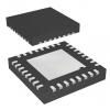
ST33HTPH2X32AHD4
STMicroelectronics
IC MCU 32BIT FLASH 32VFQFPN
CY2308SI-2
Infineon Technologies
IC FANOUT BUFFER 16SOIC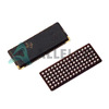
SN74LVCH32244AGKER
Texas Instruments
IC BUF NON-INVERT 3.6V 96LFBGA
HFA08TB60S
Vishay General Semiconductor - Diodes Division
DIODE GEN PURP 600V 8A TO263AB
CAT140029TWI-GT3
onsemi
IC SUPERVISOR 1 CHANNEL 8SOIC
AD7545AKRZ
Analog Devices Inc.
IC DAC 12BIT A-OUT 20SOIC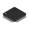
SAK-XC2030N-40F80LAA
Infineon Technologies
LEGACY 16-BIT XC2000 MCU
SI2377EDS-T1-GE3
Vishay Siliconix
MOSFET P-CH 20V 4.4A SOT23-3
STV8131
STMicroelectronics
IC REG LIN 5/8V 1A/1A 7HEPTAWATT
C3216X8R2A154M160AA
TDK Corporation
CAP CER 0.15UF 100V X8R 1206 -

VE-JW3-EY
Vicor Corporation
DC DC CONVERTER 24V 50W
MCP6409-H/SL
Microchip Technology
IC OPAMP GP 4 CIRCUIT 14SOIC
BU4215F-TR
Rohm Semiconductor
IC SUPERVISOR 1 CHANNEL 4SOP
STTH1002CR
STMicroelectronics
DIODE ARRAY GP 200V 8A I2PAK
RC4558P
Texas Instruments
IC OPAMP GP 2 CIRCUIT 8DIP
C1210X104K5RAC7800
KEMET
CAP CER 0.1UF 50V X7R 1210
DTC144TKAT146
Rohm Semiconductor
TRANS PREBIAS NPN 200MW SMT3
V300A5C400BL
Vicor Corporation
DC DC CONVERTER 5V 400W
AT25020N-10SC-2.7
Microchip Technology
IC EEPROM 2KBIT SPI 3MHZ 8SOIC
USB2512AI-AEZG
Microchip Technology
IC CTRLR USB2.0 2PORT 36QFN
1812JA101KAT1A\SB
KYOCERA AVX
CAP CER 100PF 4KV C0G/NP0 1812
ICL7660ACBA
Harris Corporation
SWITCHED CAPACITOR CONVERTER
TLV2171IDGKR
Texas Instruments
IC OPAMP GP 2 CIRCUIT 8VSSOP
D8087-1
Rochester Electronics, LLC
MATH COPROCESSOR, 16 BIT, NMOS,
GRT21BC81A226ME13L
Murata Electronics
CAP CER 22UF 10V X6S 0805
M25P64-VME6G
Micron Technology
IC FLASH 64M SPI 50MHZ 8VDFPN
CY7C2644KV18-300BZXI
Infineon Technologies
IC SRAM 144MBIT PAR 165FBGA
XR2206CP-F
MaxLinear, Inc.
IC FUNCTION GENERATOR 16DIP