View All

Please refer to the English Version as our Official Version.Return

Europe
France(Français) Germany(Deutsch) Italy(Italia) Russian(русский) Poland(polski) Czech(Čeština) Luxembourg(Lëtzebuergesch) Netherlands(Nederland) Iceland(íslenska) Hungarian(Magyarország) Spain(español) Portugal(Português) Turkey(Türk dili) Bulgaria(Български език) Ukraine(Україна) Greece(Ελλάδα) Israel(עִבְרִית) Sweden(Svenska) Finland(Svenska) Finland(Suomi) Romania(românesc) Moldova(românesc) Slovakia(Slovenská) Denmark(Dansk) Slovenia(Slovenija) Slovenia(Hrvatska) Croatia(Hrvatska) Serbia(Hrvatska) Montenegro(Hrvatska) Bosnia and Herzegovina(Hrvatska) Lithuania(lietuvių) Spain(Português) Switzerland(Deutsch) United Kingdom(English)
Asia/Pacific
Japan(日本語) Korea(한국의) Thailand(ภาษาไทย) Malaysia(Melayu) Singapore(Melayu) Vietnam(Tiếng Việt) Philippines(Pilipino)
Africa, India and Middle East
United Arab Emirates(العربية) Iran(فارسی) Tajikistan(فارسی) India(हिंदी) Madagascar(malaɡasʲ)
South America / Oceania
New Zealand(Maori) Brazil(Português) Angola(Português) Mozambique(Português)
North America
United States(English) Canada(English) Haiti(Ayiti) Mexico(español)
HomeProductsIntegrated Circuits (ICs)Linear - Amplifiers - Instrumentation, OP Amps, Buffer AmpsAD8515AKSZ-R2
AD8515AKSZ-R2 Image
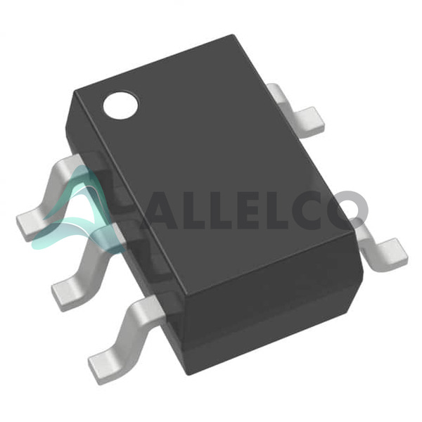
Image may be representation.
See specifications for product details.
EXPRESS OPTION
Payment method

AD8515AKSZ-R2 - Analog Devices Inc.

Manufacturer Part Number
AD8515AKSZ-R2
Manufacturer
Analog Devices, Inc.
Allelco Part Number
98D-AD8515AKSZ-R2
Warranty
1 Year Allelco Warranty - Find out more
Stock Status:
10,776 pcs available, New & Original
Parts Description
IC OPAMP GP 1 CIRCUIT SC70-5
Package
SC-70-5
Data sheet
AD8515AKSZ-R2.pdf

Datasheets

AD8515.pdf

PCN Part Status Change

Sm Reel Obs 9/Mar/2017.pdf

Other Related Documents

Tape and Reel Packaging.pdf
RoHs Status
 
Our certification
In stock: 10776

Required fields are indicated by an asterisk (*)
Please send RFQ, we will respond immediately.

Quantity

Specifications

AD8515AKSZ-R2 Tech Specifications
Analog Devices Inc. - AD8515AKSZ-R2 technical specifications, attributes, parameters and parts with similar specifications to Analog Devices Inc. - AD8515AKSZ-R2

Product Attribute Attribute Value
Manufacturer Analog Devices, Inc.
Voltage - Supply Span (Min) 1.8 V
Voltage - Supply Span (Max) 5 V
Voltage - Input Offset 1 mV
Supplier Device Package SC-70-5
Slew Rate 2.7V/µs
Series -
Package / Case 5-TSSOP, SC-70-5, SOT-353
Package Tape & Reel (TR)
Output Type Rail-to-Rail
Product Attribute Attribute Value
Operating Temperature -40°C ~ 125°C
Number of Circuits 1
Mounting Type Surface Mount
Gain Bandwidth Product 5 MHz
Current - Supply 410µA
Current - Output / Channel 20 mA
Current - Input Bias 5 pA
Base Product Number AD8515
Amplifier Type General Purpose

Environmental & Export Classifications

ATTRIBUTE DESCRIPTION
Moisture Sensitivity Level (MSL) 1 (Unlimited)
REACH Status REACH Unaffected
ECCN EAR99

Frequently Asked Questions(FAQ)

How does the AD8515AKSZ-R2 compare to other single-channel rail-to-rail op-amps in terms of power consumption and input bias current when used in low-voltage battery-powered sensor interface circuits?
The AD8515AKSZ-R2 draws 410 µA per amplifier channel, which is competitive with modern micropower op-amps like the MCP6241T-E/OT (typically 350 µA) but higher than ultra-low-power devices such as the OPA349SA/3K (around 100 µA). However, its exceptionally low input bias current of 5 pA significantly reduces long-term leakage errors in high-impedance sensor applications—advantageous over many CMOS op-amps that exhibit 1–10 nA bias currents. In a 3V battery-powered thermocouple amplifier using a 10 MΩ feedback resistor, the AD8515’s 5 pA bias current introduces less than 50 µV offset drift over time compared to potentially hundreds of microvolts with higher-bias alternatives.
What are the key limitations of the AD8515AKSZ-R2 when driving capacitive loads above 100 nF in precision data acquisition systems, and how do these compare to similar general-purpose amplifiers?
The AD8515AKSZ-R2 has limited phase margin under heavy capacitive loading, which can lead to instability or ringing when driving loads exceeding approximately 100 nF without series resistance. This behavior is typical of many general-purpose op-amps with moderate slew rates like 2.7 V/µs. Compared to more robust load-driving amplifiers such as the ISL28114FEZ-T7A, which features internal compensation and higher output current drive (up to 40 mA), the AD8515 requires external isolation resistors (e.g., 22 Ω) in series with the load to maintain stability. Failure to include this resistor may result in transient oscillations during fast step responses, particularly problematic in sample-and-hold or active-filter stages where signal integrity is critical.
Can the AD8515AKSZ-R2 be safely used in automotive temperature sensing applications spanning -40°C to +125°C, considering input offset voltage drift and long-term reliability?
Yes, the AD8515AKSZ-R2 is specified for industrial-grade operation from -40°C to +125°C, making it suitable for automotive environments within that range. Its input offset voltage of 1 mV at 25°C increases with temperature; typical drift is around 5 µV/°C, resulting in a total offset variation of ±125 µV across the full temperature span—manageable in most analog front-end designs. However, users should verify solder joint integrity under thermal cycling, especially given the small SC-70-5 package. While not AEC-Q100 qualified, many designers successfully deploy this part in non-safety-critical automotive auxiliary sensing due to Analog Devices’ consistent quality processes and Moisture Sensitivity Level 1 handling requirements.
What is the effective bandwidth of the AD8515AKSZ-R2 when configured as a transimpedance amplifier with a 1 MΩ feedback resistor and photodiode capacitance of 150 pF?
In a typical transimpedance configuration using a 1 MΩ resistor and 150 pF photodiode capacitance, the dominant pole is set by R_f × C_load = 1 MΩ × 150 pF = 150 kHz. The AD8515’s gain-bandwidth product of 5 MHz implies unity-gain bandwidth, so the closed-loop bandwidth becomes approximately 1 / (2π × R_f × C_total). Accounting for op-amp input capacitance (~3 pF) and stray layout parasitics, the actual bandwidth drops to roughly 100–120 kHz. This limits the maximum achievable conversion speed for low-light photodetection unless compensated with T-network feedback or reduced R_f, trading sensitivity for bandwidth.
How does the output swing performance of the AD8515AKSZ-R2 differ between 2.5V and 5V supply rails, and what impact does this have on rail-to-rail ADC interfacing?
At a 5V supply, the AD8515 typically delivers within 10 mV of each rail, enabling full-scale output swing for 12-bit ADCs referenced to 5V. However, at 2.5V supply, output swing degrades—often reaching only ~20 mV below V+ and ~30 mV above V− due to internal architecture constraints. This asymmetry affects bidirectional signal paths. When driving a 1.8V ADC input from a 2.5V system, headroom is severely limited; for example, an input swing of ±100 mV yields output levels between 2.37 V and 2.4 V, reducing dynamic range by nearly half compared to a 5V rail scenario. Designers must account for this when selecting reference voltages or scaling factors.
Is the AD8515AKSZ-R2 suitable for use in precision DC-coupled instrumentation amplifiers requiring better than 10 µV/V gain accuracy over 100:1 dynamic range?
No, the AD8515AKSZ-R2 lacks the precision characteristics needed for high-accuracy DC measurements. With a gain-bandwidth product of only 5 MHz and slew rate of 2.7 V/µs, it cannot support wide dynamic ranges without introducing settling errors. Moreover, its input offset voltage of 1 mV and drift of 5 µV/°C translate into gain errors exceeding 100 µV/V even in buffered configurations, far above the 10 µV/V target. Alternatives like the OPA349SA/3K offer lower offset and better linearity, while dedicated instrumentation amplifiers such as the INA128 provide superior CMRR and precision. The AD8515 remains better suited for moderate-speed, cost-sensitive switching or conditioning tasks rather than precision amplification.
What precautions should be taken when laying out PCBs for the AD8515AKSZ-R2 to minimize parasitic coupling and ensure stability in mixed-signal environments?
Due to the SC-70-5’s small size and high input impedance, the AD8515AKSZ-R2 is sensitive to layout parasitics. Power supplies must be bypassed with 100 nF capacitors placed within 1 mm of the device pins. Feedback networks should use low-tolerance, stable resistors (≤1%) and avoid long traces that introduce inductance. Ground return paths must be minimized, and analog ground planes should connect directly to digital grounds at a single point near the supply entry. Additionally, guard rings or careful trace spacing help mitigate leakage currents in humid conditions. These practices prevent oscillation and noise pickup, particularly important given the part’s 2.7 V/µs slew rate, which makes it susceptible to fast transients.
How does the AD8515AKSZ-R2 perform in single-supply battery monitoring circuits with input signals crossing ground, and what protection mechanisms are necessary?
The AD8515AKSZ-R2 supports single-supply operation down to 1.8 V and accepts input voltages beyond the negative rail by up to 200 mV, allowing true ground-crossing inputs in single-ended configurations. For example, in a 3V battery monitor detecting loads drawing negative transients, the input can go slightly below ground without damage. However, external Schottky diodes from each input pin to the supply rails are recommended to clamp any sustained overvoltage events, as internal ESD structures may not protect against repeated excursions. Without such clamping, repeated undershoots could accumulate charge on junction capacitances, degrading performance over time—unlike more robust I/O tolerant devices like the MCP6241T-E/OT, which includes integrated diode clamps.
What is the maximum allowable capacitive load before instability occurs in unity-gain buffer mode using the AD8515AKSZ-R2, and how does this compare to other general-purpose amplifiers?
The AD8515AKSZ-R2 becomes unstable with capacitive loads above approximately 300 pF in unity-gain buffer configuration due to insufficient phase margin. Adding a small series resistor (e.g., 22 Ω) isolates the capacitor and restores stability. In comparison, the OPA349SA/3K tolerates loads up to 1 µF without modification, while the MCP6241T-E/OT handles about 500 pF. The AD8515’s lower slew rate and moderate GBW limit its drive capability in buffer roles. Thus, in precision ADC driver applications requiring large hold capacitors (>400 pF), alternative amplifiers with built-in compensation or higher output drive are preferable unless external isolation is implemented.
How does the AD8515AKSZ-R2 handle common-mode voltage variations when used in differential-to-single-ended conversion for noisy industrial environments?
The AD8515AKSZ-R2 accepts input common-mode voltages from –0.2 V to V+ + 0.2 V, allowing operation near the negative rail. In a 3V system monitoring a 0–3V sensor output, the full range is usable without level shifting. However, its CMRR is modest (~80 dB typ.), limiting rejection of differential noise in unbalanced lines. For improved performance, matched gain resistors (within 0.1%) and careful layout are essential. Compared to precision op-amps like the ISL28114FEZ-T7A (CMRR >90 dB), the AD8515 offers adequate but not exceptional common-mode suppression. Therefore, in electrically noisy settings with long cable runs, additional filtering or instrumentation amplifiers are advised unless signal conditioning precedes the AD8515 stage.
What are the implications of using the AD8515AKSZ-R2 in switched-capacitor filter applications requiring precise timing and minimal settling error?
The AD8515AKSZ-R2’s 2.7 V/µs slew rate and 5 MHz GBW restrict its suitability for high-order switched-capacitor filters demanding fast settling. For instance, in a 10th-order elliptic filter with 10 kSPS throughput, each sample window may require multiple clock cycles to settle fully. Given its typical settling time to 0.1% for a 10 V step is about 1.5 µs, achieving reliable performance above 300 kSPS is challenging. While usable in first- or second-order sigma-delta modulators at moderate speeds, designs targeting >1 MSPS should consider faster op-amps like those with 10 V/µs slew rates. The AD8515 remains viable for lower-data-rate applications where cost and power dominate over speed.
How does the base product family (AD8515) differentiate itself from similar general-purpose amplifiers like the MCP6241T-E/OT and OPA349SA/3K in terms of noise and dynamic range?
The AD8515AKSZ-R2 exhibits input-referred voltage noise of ~40 nV/√Hz, comparable to the MCP6241T-E/OT but higher than the OPA349SA/3K (~30 nV/√Hz). However, its lower input bias current (5 pA vs. ~1 nA for MCP6241) reduces low-frequency flicker noise contributions in high-impedance sources. In a 1 kHz bandwidth measurement system, the AD8515 contributes approximately 1.3 µV RMS noise, sufficient for 12-bit resolution but marginal for 16-bit systems without averaging. Its 5 MHz GBW enables wider signal capture than slower devices but trades off precision for speed—making it ideal for applications where both moderate bandwidth and ultralow leakage are required, such as battery-backed sensor nodes.
What design trade-offs arise when substituting the AD8515AKSZ-R2 for the AD8515AKSZ-REEL7 in production volumes, and how might packaging affect thermal performance?
The AD8515AKSZ-R2 is tape-and-reel packaged for automated assembly, while the AD8515AKSZ-REEL7 denotes the same part in reel form. Both share identical electrical specifications and SC-70-5 footprint. However, handling differences during SMT placement can affect yield if feeder alignment is inconsistent. Thermal performance is nearly identical due to shared package construction; neither variant benefits significantly from heatsinking. In high-ambient-temperature environments (>85°C), junction temperatures may approach limits during continuous 20 mA output swings, but typical signal levels keep self-heating negligible. Substitution between these variants is seamless provided PCB pads and reflow profiles match manufacturer recommendations.
Can the AD8515AKSZ-R2 be used in audio preamplifier stages for MEMS microphones operating at 1.8V supply, and what signal-to-noise considerations apply?
Yes, the AD8515AKSZ-R2 supports 1.8V operation and can amplify sub-millivolt signals from MEMS microphones with appropriate gain staging. However, its 40 nV/√Hz input noise density limits dynamic range in quiet environments. For a -32 dBV microphone signal (≈2.5 mVpp), the SNR is approximately 70 dB in 20 kHz bandwidth—adequate for voice recognition but insufficient for music reproduction. Additionally, the 1 mV input offset may require AC-coupling or trimming in fixed-gain designs. While functional, dedicated low-noise audio op-amps like the ADA4061 offer better performance at similar supply voltages, making the AD8515 a compromise between cost, power, and functionality.
What is the expected lifetime and failure rate for the AD8515AKSZ-R2 under continuous 25°C operation with 2.5V supply and typical output current draw?
Under continuous operation at 25°C with 2.5V supply and 5 mA average output current, the AD8515AKSZ-R2 experiences minimal stress. Based on Analog Devices’ reliability models and Arrhenius analysis, FIT (Failures In Time) rates are estimated below 10 FITs for this usage profile. Assuming a mission time of 10 years (87,600 hours), the predicted failure probability is <0.1%. This assumes proper PCB layout, no electrostatic discharge events, and adherence to absolute maximum ratings. Actual field life exceeds 20 years in most consumer and industrial applications, reinforcing its robustness for long-duration embedded systems.
How does the AD8515AKSZ-R2 compare to the MCP6241T-E/OT in terms of input offset drift and suitability for battery voltage measurement over extended temperature cycles?
The AD8515AKSZ-R2 exhibits 5 µV/°C input offset drift, whereas the MCP6241T-E/OT typically shows 3 µV/°C. Over a 100°C range, the AD8515 introduces up to 500 µV offset shift, sufficient to cause 0.02% error in a 2.5V battery reading—acceptable for most monitoring apps. However, the MCP6241’s slightly better drift and lower quiescent current (350 µA vs. 410 µA) make it marginally superior in ultra-low-power battery monitors. Still, both parts operate reliably from 1.8V to 5V, and the AD8515’s lower input bias current gives it an edge in high-impedance divider networks, reducing loading effects on resistive voltage dividers.
What precautions are necessary when storing or transporting the AD8515AKSZ-R2 to prevent moisture-induced failures despite its MSL 1 classification?
Although the AD8515AKSZ-R2 has Moisture Sensitivity Level 1 (unlimited floor life), it must still be stored in dry environments (<30% RH) to prevent condensation during rapid temperature changes—especially in humid climates or after exposure to refrigeration. Standard anti-static bags with desiccant are recommended. During transport, avoid prolonged exposure to salt spray or high-humidity warehouses. While delamination risk is low due to the SC-70-5’s thin mold compound, sudden humidity spikes can cause popcorn effect during reflow if absorbed moisture exceeds 0.1% weight gain. Routine visual inspection post-opening ensures reliability, particularly in coastal or tropical manufacturing facilities.
In what scenarios would replacing the AD8515AKSZ-R2 with the ISL28114FEZ-T7A improve system performance, and what key parameters justify this substitution?
Replacing the AD8515AKSZ-R2 with the ISL28114FEZ-T7A is beneficial when higher output current drive (up to 40 mA vs. 20 mA) and improved capacitive load stability are required. The ISL28114 also offers lower input voltage noise (35 nV/√Hz) and better rail-to-rail output swing near rails, enhancing signal fidelity in driving long cables or active filters. Additionally, its internal compensation allows stable operation with loads up to 1 µF without external resistors, simplifying layout. Use the substitution in applications like motor control feedback loops or multi-stage active filters where the AD8515’s limitations in drive strength or phase margin become bottlenecks.

Parts with Similar Specifications

The three parts on the right have similar specifications to Analog Devices Inc. AD8515AKSZ-R2

Product Attribute AD8515AKSZ-REEL7 AD8515AKSZR2 AD8515AKS-R2 AD8515AKS-REEL7
Part Number AD8515AKSZ-REEL7 AD8515AKSZR2 AD8515AKS-R2 AD8515AKS-REEL7
Manufacturer Analog Devices Inc. Analog Devices Inc. Analog Devices Inc. Analog Devices Inc.
Operating Temperature - -40°C ~ 85°C 0°C ~ 70°C -40°C ~ 85°C
Supplier Device Package - 196-NFBGA (12x12) 16-PDIP 64-VQFN (9x9)
Amplifier Type - - - -
Number of Circuits - - - -
Voltage - Supply Span (Min) - - - -
Package - Tape & Reel (TR) Tube Tape & Reel (TR)
Current - Input Bias - - - -
Base Product Number - DAC34H84 MAX500 ADS62P42
Current - Output / Channel - - - -
Voltage - Input Offset - - - -
Mounting Type - Surface Mount Through Hole Surface Mount
Package / Case - 196-LFBGA 16-DIP (0.300', 7.62mm) 64-VFQFN Exposed Pad
Gain Bandwidth Product - - - -
Output Type - Current - Unbuffered Voltage - Buffered -
Slew Rate - - - -
Series - - - -
Current - Supply - - - -
Voltage - Supply Span (Max) - - - -

AD8515AKSZ-R2 Datasheet PDF

Download AD8515AKSZ-R2 pdf datasheets and Analog Devices Inc. documentation for AD8515AKSZ-R2 - Analog Devices Inc..

Datasheets
AD8515.pdf
PCN Part Status Change
Sm Reel Obs 9/Mar/2017.pdf
Other Related Documents
Tape and Reel Packaging.pdf
Design Resources
Extending the Capacitive Input Range of AD7745/AD7.pdf

Customer Reviews

Evaluation: 10 Articles

  • Nath***rooks
    Jun 11, 2026

    Installed this power component in a converter board. Output remained stable under different load conditions and thermal performance was better than expected.

  • Dani***alkerTech
    Jun 1, 2026

    Product works, but setup took more effort than expected. Once configured the MCU ran reliably, although documentation support felt older compared with newer platforms. Fine for maintenance projects.

  • Yuki***aka88
    May 26, 2026

    信号通信プロジェクトでこのRS-485トランシーバーを使用しました。設置は簡単で、長距離ケーブルでも通信は安定していました。消費電力も、以前使用していたものより低くなっています。

  • Stev***aker
    May 20, 2026

    Solid diode for power rectification. Works well in switching circuits.

  • Bran***Lewis
    May 11, 2026

    Compact FPGA with good performance. Suitable for basic signal processing tasks.

  • Oliv***arris
    May 7, 2026

    Reliable I/O expander. Works well in embedded control applications.

  • Jess***Jones
    Apr 17, 2026

    It offers good value for the price, and the specifications match the description. I’ve been using it for two days with no issues, and I’ll definitely buy it again if I need it in the future.

  • Mich***Smith
    Apr 17, 2026

    Shipping was on time, the component pins are neatly aligned, and I tested 10 of them with a multimeter—all readings were within the specified range. Highly recommended.

  • Aman***arris
    Apr 3, 2026

    It was great—the entire process, from placing the order to receiving the package, went very smoothly. The components were consistent, the price was fair, and I had a very pleasant shopping experience.

  • Mike***nch
    Apr 3, 2026

    Better than expected! The resistance and capacitance readings were spot-on, and it passed the test on the first try. The service was reliable, and the packaging was thoughtful—I highly recommend it.

Write a Review

Your Email address will not be published.

Shipment

Delivery Time

In-stock items can be shipped within 24 hours. Some parts will be arranged for delivery within 1-2 days from the date all items arrive at our warehouse. And Allelco ships order once a day at about 17:00, except Sunday. Once the goods are shipped, the estimated delivery time depends on the shipping methods and Delivery destination. The table below shows are the logistic time for some common countries.

Delivery Cost

  1. Use your express account for shipment if you have one.
  2. Use our account for the shipment. Refer to the table below for the approximate charges.
(Different time frame / countries / package size has different price.)

Delivery Method

  1. Global Common Shipment by DHL / UPS / FedEx / TNT / EMS / SF we support.
  2. Others more shipping ways, please get in touch with your customer manager.

Common Countries Logistic Time Reference
Region Country Logistic Time(Day)
America United States 5
Brazil 7
Europe Germany 5
United Kingdom 4
Italy 5
Oceania Australia 6
New Zealand 5
Asia India 4
Japan 4
Middle East Israel 6
DHL & FedEx Shipment Charges Reference
Shipment charges(KG) Reference DHL(USD$)
0.00kg-1.00kg USD$30.00 - USD$60.00
1.00kg-2.00kg USD$40.00 - USD$80.00
2.00kg-3.00kg USD$50.00 - USD$100.00
Note:
The above table is for reference only. There may have some data bias for the uncontrollable factors.
Contact us if you have any questions.
  • QC (Quality Warranty)
  • Payment Support
  • Packaging
  • Certifications & Memberships

QC (Quality Warranty)

Allelco is committed to exceeding customer expectations through customer service excellence, order accuracy, and on-time delivery.
This is achieved through our commitment to the continual improvement of our processes, services, and products.


Strict quality inspection builds a solid foundation for electronic component quality.
  1. Visual inspection
  2. Performance testing and reliability verification
  3. Standardized full-process testing
  4. Precise control of every parameter
We eliminate defective components and ensure the stable operation of electronic devices through professional quality standards.

Payment Support

The payment method can be chosen from the methods shown below: Wire Transfer (T/T, Bank Transfer), Western Union, Credit card, PayPal.
  • HKBea
  • Paypal
  • MasterCard
  • Western-Union
  • VISA
Stable Delivery, Sincere Partnership — Your Faithful Supply Chain Partner
  • Efficient Supply Management
  • Cost-Saving Procurement
  • Fast Sourcing & Delivery
Contact us if you have any questions.

Packaging

Electrostatic Discharge Protection and Handling

All electrostatic-sensitive components are handled in accordance with electrostatic discharge control procedures. The products are hermetically sealed in anti-static safe packaging to prevent electrostatic damage. Appropriate labeling is also applied for identification and traceability. This ensures product integrity during storage, handling and transportation.


ESD

Certifications & Memberships

Third-party certified, strict quality control. Our certification
  • ISO 9001: 2015
  • ISO 13485: 2016
  • ISO 14001: 2015
  • ISO 28000: 2007
  • ISO 45001: 2018
  • GB/T 27922-2011
  • SMTA
  • IPC
  • ESD
  • PSMA
AD8515AKSZ-R2 Image

AD8515AKSZ-R2

Analog Devices Inc.
98D-AD8515AKSZ-R2

Want a better price? Add to Cart and Submit RFQ now, we'll contact you immediately.

0 RFQ
Shopping cart (0 Items)
It is empty.
Compare List (0 Items)
It is empty.
Feedback

Your feedback matters! At Allelco, we value the user experience and strive to improve it constantly.
Please share your comments with us via our feedback form, and we'll respond promptly.
Thank you for choosing Allelco.

Subject
E-mail
Comments
Captcha
Drag or click to upload file
Upload File
types: .xls, .xlsx, .doc, .docx, .jpg, .png and .pdf.
Max file size: 10MB