
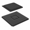
Manufacturer Part Number
XC2VP7-5FF896C
Manufacturer
Xilinx
Introduction
The XC2VP7-5FF896C is a Virtex-II Pro FPGA from Xilinx, designed for embedded applications. It offers a high-performance, feature-rich platform with configurable logic blocks, embedded PowerPC processors, and advanced I/O capabilities.
Product Features and Performance
1232 Configurable Logic Blocks (CLBs) with 11,088 logic cells
811,008 total RAM bits
396 user I/O pins
Operating voltage of 1.425V to 1.575V
Operating temperature range of 0°C to 85°C
896-pin Ball Grid Array (BGA) package
Product Advantages
Powerful and flexible FPGA architecture for a wide range of embedded applications
Embedded PowerPC processors for high-performance computing
Extensive on-chip memory and advanced I/O capabilities
Configurable and reconfigurable design
Key Reasons to Choose This Product
Robust and reliable FPGA solution from a leading manufacturer
Suitable for a variety of embedded applications requiring high-performance and flexibility
Versatile architecture that can be customized to meet specific design requirements
Proven track record and support from Xilinx
Quality and Safety Features
Rigorous testing and quality control processes
Compliance with industry standards and regulations
Thermal management features for reliable operation
Compatibility
Compatible with Xilinx's comprehensive design tools and software ecosystem
Supports integration with a wide range of peripherals and interface standards
Application Areas
Embedded systems
Industrial automation and control
Telecommunications
Medical devices
Military and aerospace applications
Product Lifecycle
This product is currently in the Obsolete status, meaning it is no longer in active production. However, there are several alternative and equivalent Virtex-II Pro FPGA models available from Xilinx, such as the XC2VP20, XC2VP30, and XC2VP50, which offer similar or enhanced capabilities. Customers are advised to contact our website's sales team for more information on available options and support for the XC2VP7-5FF896C or its alternatives.
 XC2VP7-5FG456CAMDIC FPGA 248 I/O 456FBGA
 XC2VP50-6FFG1517IXilinx Inc.IC FPGA 852 I/O 1517FCBGA
 XC2VP50-7FF1148CXilinx Inc.IC FPGA 812 I/O 1148FCBGA
 XC2VP50-7FF1152CAMDIC FPGA 692 I/O 1152FCBGA
 XC2VP7-5FFG896CXILINX


