
XC2VP7-5FG456I (1)
Manufacturer Part Number
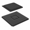
XC2VP7-5FG456I
Manufacturer
Xilinx
Introduction
Xilinx Virtex-II Pro FPGA integrated circuit for advanced embedded applications
Product Features and Performance
1232 LABs/CLBs for logic processing
11088 Logic Elements/Cells for complex design implementation
811008 Total RAM Bits for high-capacity memory storage
248 I/O pins for versatile connectivity
Surface Mount technology compatible
456-BBGA package for robust physical integration
Supports a wide range of supply voltage (1.425V ~ 1.575V)
Product Advantages
High logic capacity for demanding applications
Extensive memory resources
High pin count for interfacing flexibility
Operational across wide temperature range -40°C ~ 100°C
Key Technical Parameters
Total Number of LABs/CLBs: 1232
Logic Elements/Cells: 11088
Total RAM Bits: 811008
Number of I/O: 248
Voltage - Supply Range: 1.425V ~ 1.575V
Operating Temperature Range: -40°C ~ 100°C
Quality and Safety Features
Built-in features for enhanced reliability and performance
Compliance with industry quality and safety standards
Compatibility
Compatible with various design environments due to high I/O count
Application Areas
Suitable for complex, embedded processing in telecommunications, industrial, and more
Product Lifecycle
Obsolete status with potential limited availability
Consider alternatives for replacements or upgrades
Several Key Reasons to Choose This Product
Highly integrated FPGA solution
Robust performance over an extended temperature range
Ideal for complex digital processing tasks
Xilinx support and reliability
 XC2VP7-6FFG672IAMDIC FPGA 396 I/O 672FCBGA
 XC2VP7-6FFG896CAMDIC FPGA 396 I/O 896FCBGA
 XC2VP7-5FF896CAMDIC FPGA 396 I/O 896FCBGA


