XC2VP7-6FFG672C (1)
Manufacturer Part Number
XC2VP7-6FFG672C
Manufacturer
Xilinx
Introduction
The Xilinx XC2VP7-6FFG672C is a high-performance, field-programmable gate array (FPGA) from the Virtex-II Pro series. It is designed for a wide range of embedded applications, offering a balance of logic resources, on-chip memory, and high-speed serial transceivers.
Product Features and Performance
1232 logic cells (CLBs) and 11,088 logic elements
811,008 total RAM bits
396 user-programmable I/O pins
Operates at a supply voltage of 1.425V to 1.575V
Operating temperature range of 0°C to 85°C (junction temperature)
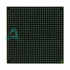
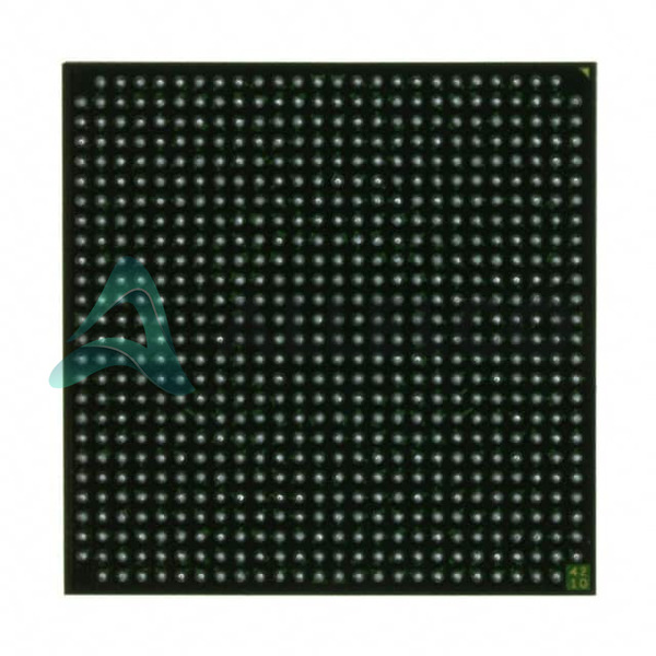
672-pin BBGA (Ball Grid Array) package, 27x27 mm size
Product Advantages
Versatile and reconfigurable architecture for flexible design implementation
Optimized for high-performance, low-power embedded applications
Integrated serial transceivers for high-speed data communication
Extensive on-chip memory resources for data buffering and processing
Key Reasons to Choose This Product
Powerful FPGA capabilities with a robust feature set
Proven Virtex-II Pro technology for reliable and efficient performance
Scalable solution for a wide range of embedded system requirements
Supports rapid prototyping and design flexibility
Quality and Safety Features
Rigorously tested and validated to meet Xilinx's quality standards
Designed with robust power management and thermal considerations
Supports various safety-critical applications through advanced features
Compatibility
The XC2VP7-6FFG672C is compatible with the Virtex-II Pro series of FPGAs and can be used in a variety of embedded systems and applications.
Application Areas
Industrial automation and control systems
Medical imaging and instrumentation
Telecommunications and networking equipment
Military and defense applications
Scientific and research equipment
Product Lifecycle
The XC2VP7-6FFG672C is an obsolete product, meaning it is no longer in active production. However, there are several equivalent and alternative Virtex-II Pro FPGA models available from Xilinx that may be suitable replacements. If you require more information or assistance in finding a suitable alternative, please contact our website's sales team.
 XC2VP7-6FG456CAMDIC FPGA 248 I/O 456FBGA
 XC2VP7-6FF896IAMDIC FPGA 396 I/O 896FCBGA
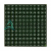 XC2VP7-5FFG896IXilinxIC FPGA 396 I/O 896FCBGA
 XC2VP7-6FGG456CXILINX


