 XC2VP7-6FFG896CAMDIC FPGA 396 I/O 896FCBGA
 XC2VP7-5FFG896IXilinxIC FPGA 396 I/O 896FCBGA
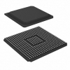 XC2VP7-6FG456IAMDIC FPGA 248 I/O 456FBGA
 XC2VP7-6FFG896IXILINX
- Nath***rooks
- Jun 11, 2026
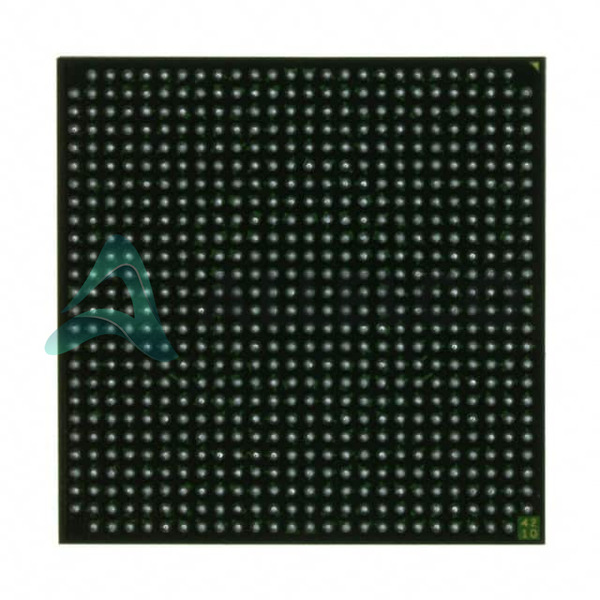
Image may be representation.
See specifications for product details.
See specifications for product details.
- EXPRESS OPTION
- Payment method
XC2VP7-6FF672I - AMD
- Manufacturer Part Number
- XC2VP7-6FF672I
- Manufacturer
- AMD Xilinx
- Allelco Part Number
- 98D-XC2VP7-6FF672I
- Warranty
- 1 Year Allelco Warranty - Find out more
- Stock Status:
- 16,490 pcs available, New & Original
- Parts Description
- IC FPGA 396 I/O 672FCBGA
- Package
- 672-FCBGA (27x27)
- Data sheet
-
XC2VP7-6FF672I.pdf
Datasheets
Virtex-II Pro, Pro X.pdfPCN Obsolescence/ EOL
Mult Dev EOL 6/Jan/2020.pdfEnvironmental Information
Xilinx REACH211 Cert.pdf
- RoHs Status
- Our certification
- In stock: 16490


