View All

Please refer to the English Version as our Official Version.Return

Europe
France(Français) Germany(Deutsch) Italy(Italia) Russian(русский) Poland(polski) Czech(Čeština) Luxembourg(Lëtzebuergesch) Netherlands(Nederland) Iceland(íslenska) Hungarian(Magyarország) Spain(español) Portugal(Português) Turkey(Türk dili) Bulgaria(Български език) Ukraine(Україна) Greece(Ελλάδα) Israel(עִבְרִית) Sweden(Svenska) Finland(Svenska) Finland(Suomi) Romania(românesc) Moldova(românesc) Slovakia(Slovenská) Denmark(Dansk) Slovenia(Slovenija) Slovenia(Hrvatska) Croatia(Hrvatska) Serbia(Hrvatska) Montenegro(Hrvatska) Bosnia and Herzegovina(Hrvatska) Lithuania(lietuvių) Spain(Português) Switzerland(Deutsch) United Kingdom(English)
Asia/Pacific
Japan(日本語) Korea(한국의) Thailand(ภาษาไทย) Malaysia(Melayu) Singapore(Melayu) Vietnam(Tiếng Việt) Philippines(Pilipino)
Africa, India and Middle East
United Arab Emirates(العربية) Iran(فارسی) Tajikistan(فارسی) India(हिंदी) Madagascar(malaɡasʲ)
South America / Oceania
New Zealand(Maori) Brazil(Português) Angola(Português) Mozambique(Português)
North America
United States(English) Canada(English) Haiti(Ayiti) Mexico(español)
HomeProductsIntegrated Circuits (ICs)Embedded - MicrocontrollersLM3S300-IQN25-C2
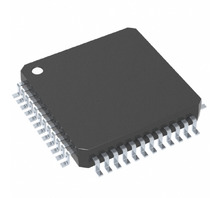
LM3S300-IQN25-C2 Image
Image may be representation.
See specifications for product details.
EXPRESS OPTION
Payment method

LM3S300-IQN25-C2 - Texas Instruments

Manufacturer Part Number
LM3S300-IQN25-C2
Manufacturer
Texas Instruments
Allelco Part Number
32D-LM3S300-IQN25-C2
Warranty
1 Year Allelco Warranty - Find out more
Stock Status:
4,233 pcs available, New & Original
Parts Description
IC MCU 32BIT 16KB FLASH 48LQFP
Package
48-LQFP (7x7)
Data sheet
LM3S300-IQN25-C.pdf

PCN Assembly/Origin

Assembly 23/Feb/2021.pdf
RoHs Status
ROHS3 Compliant
Our certification
In stock: 4233

Required fields are indicated by an asterisk (*)
Please send RFQ, we will respond immediately.

Quantity

Specifications

LM3S300-IQN25-C2 Tech Specifications
Texas Instruments - LM3S300-IQN25-C2 technical specifications, attributes, parameters and parts with similar specifications to Texas Instruments - LM3S300-IQN25-C2

Product Attribute Attribute Value
Manufacturer Texas Instruments
Voltage - Supply (Vcc/Vdd) 3V ~ 3.6V
Supplier Device Package 48-LQFP (7x7)
Speed 25MHz
Series Stellaris® ARM® Cortex®-M3S 300
RAM Size 4K x 8
Program Memory Type FLASH
Program Memory Size 16KB (16K x 8)
Peripherals Brown-out Detect/Reset, POR, PWM, WDT
Package / Case 48-LQFP
Package Tray
Product Attribute Attribute Value
Oscillator Type Internal
Operating Temperature -40°C ~ 85°C (TA)
Number of I/O 36
Mounting Type Surface Mount
EEPROM Size -
Data Converters -
Core Size 32-Bit Single-Core
Core Processor ARM® Cortex®-M3
Connectivity I²C, Microwire, SPI, SSI, UART/USART
Base Product Number LM3S300

Environmental & Export Classifications

ATTRIBUTE DESCRIPTION
RoHs Status ROHS3 Compliant
Moisture Sensitivity Level (MSL) 3 (168 Hours)
REACH Status REACH Unaffected
ECCN EAR99
HTSUS 8542.31.0001

Parts Introduction

LM3S300-IQN25-C2 Image
LM3S300-IQN25-C2 (1)

Manufacturer Part Number

LM3S300-IQN25-C2

Manufacturer

Texas Instruments

Introduction

The LM3S300-IQN25-C2 is part of the Stellaris ARM Cortex-M3S 300 series, designed for embedded microcontroller applications. It utilizes a 32-bit single-core ARM Cortex-M3 processor.

Product Features and Performance

32-bit ARM Cortex-M3 core processor with a speed of 25MHz

Connectivity includes I2C, Microwire, SPI, SSI, UART/USART

Features Brown-out Detect/Reset, Power-on Reset (POR), Pulse Width Modulation (PWM), Watchdog Timer (WDT)

Internal oscillator

36 I/O pins

Product Advantages

Efficient processing with ARM Cortex-M3 core contributing to better real-time operation

Adequate speed for a variety of basic embedded systems

Multiple connectivity options for enhanced interfacing capabilities

Equipped with critical peripherals supporting system reliability and safety

Key Technical Parameters

Core Size: 32-Bit Single-Core

Speed: 25MHz

Program Memory Size: 16KB (16K x 8)

RAM Size: 4K x 8

Voltage Supply (Vcc/Vdd): 3V to 3.6V

Temperature Range: -40°C to 85°C

Mounting Type: Surface Mount

Packaging: 48-LQFP (7x7)

Quality and Safety Features

Embracement of critical safety peripherals like Brown-out Detect/Reset and Watchdog Timer

Compatibility

Compatible with a broad range of external components through its multiple connectivity interfaces

Application Areas

Suitable for light-weight embedded systems across various sectors, including consumer electronics, automation, and IoT devices

Product Lifecycle

Marked as Not For New Designs, indicating that it may be near end-of-life with potential for discontinuation and replacement suggestions to be considered

Several Key Reasons to Choose This Product

Reliability through integrated safety features

Flexibility in design with assorted connectivity options

Proven core architecture (ARM Cortex-M3) delivering robust performance for embedded applications

Availability in industrial temperature ranges, facilitating deployment in varied environments

Surface mount package supporting compact and efficient designs
Frequently Asked Questions(FAQ)

How does the LM3S300-IQN25-C2 compare to other Stellaris Cortex-M3 devices in terms of flash memory and clock speed when used in low-power embedded applications?
The LM3S300-IQN25-C2 features 16KB of on-chip flash memory and operates at a maximum clock speed of 25MHz, which positions it as a mid-tier option within the Stellaris Cortex-M3 family. While some variants in the same series offer up to 256KB of flash, they typically require external crystal oscillators for higher timing precision, increasing system complexity and power consumption. In contrast, the LM3S300-IQN25-C2 uses an internal oscillator, reducing component count and supporting faster time-to-market for space-constrained designs. For applications where moderate code size and deterministic performance are prioritized over ultra-high throughput, this balance makes the LM3S300-IQN25-C2 a practical choice, especially when operating within its 3V–3.6V supply range.
What are the key limitations of using the LM3S300-IQN25-C2 in real-time control systems requiring precise timing?
The LM3S300-IQN25-C2 relies on an internal oscillator with typical accuracy of ±1% to ±2%, which may not meet stringent timing requirements in high-precision motor control or sensor sampling applications. This limitation arises because internal oscillators are sensitive to temperature drift and manufacturing variations, potentially causing jitter in UART baud rates or PWM duty cycles. While the device includes peripherals like SSI and SPI for reliable communication, users should validate timing margins under worst-case temperature conditions (-40°C to 85°C). For such applications, pairing the LM3S300-IQN25-C2 with an external 4–20 MHz crystal improves stability but increases board area and cost.
Can the LM3S300-IQN25-C2 support multiple UART interfaces simultaneously without significant overhead?
Yes, the LM3S300-IQN25-C2 provides four UART/USART channels, enabling concurrent serial communication with minimal CPU overhead. With a 25MHz core clock, each UART can operate at standard baud rates such as 115200 bps using integer oversampling, ensuring accurate framing even at higher speeds. However, simultaneous operation across all four channels may increase interrupt load, particularly if echo handling or flow control is implemented. Developers should consider using DMA (if available via peripheral extensions) or prioritizing critical communications to maintain responsiveness. This capability makes the LM3S300-IQN25-C2 suitable for multi-device networking in industrial automation setups.
Is the 4K x 8 RAM sufficient for implementing complex state machines or buffering data from multiple sensors?
The 32K-bit (4K x 8) SRAM limits the LM3S300-IQN25-C2 to lightweight buffering and moderate state machine complexity. For example, buffering three analog inputs sampled at 1 kHz with 10-bit resolution would consume approximately 30 bytes, leaving ample headroom. However, storing large datasets—such as waveform capture or multi-channel logging—would quickly exhaust memory. Applications requiring deep FIFO queues or runtime data processing should avoid relying solely on internal RAM. Instead, designers can leverage the FLASH’s fast read access for lookup tables or use external SRAM via SSI/SPI if expandability is essential.
How does the operating voltage range of 3V to 3.6V affect compatibility with common battery-powered systems?
The LM3S300-IQN25-C2’s 3V–3.6V operating range aligns well with single-cell lithium-ion batteries (nominal 3.7V, dropping to ~3V at end-of-life), making it ideal for portable devices. However, it cannot directly interface with alkaline AA cells that drop below 2V during discharge. Users must implement a step-up regulator or switch to LiPo chemistry to maintain stable operation. Additionally, at lower voltages near 3.0V, the internal oscillator frequency may drift slightly, necessitating calibration routines in time-sensitive firmware. This voltage window also ensures compatibility with 3.3V logic levels, simplifying I/O interfacing.
What considerations apply when selecting between LQFP and QFN packages for production runs involving the LM3S300-IQN25-C2?
The LM3S300-IQN25-C2 is available in a 48-LQFP (7x7 mm) package, which offers superior thermal dissipation and easier manual assembly compared to smaller QFN alternatives. However, the LQFP’s exposed leads increase risk of short circuits during reflow if solder bridging occurs, requiring careful PCB design with adequate spacing and solder paste control. For high-volume production, the LQFP supports automated optical inspection (AOI) more reliably than fine-pitch QFNs. Thermal performance is adequate given the modest power envelope (~50 mW typical), but designers should ensure proper copper pour connections beneath the package to mitigate junction temperatures above 70°C during sustained loads.
Are there known issues with flash memory endurance or data retention for the LM3S300-IQN25-C2 in long-term deployments?
Texas Instruments specifies flash memory endurance of 10,000 write/erase cycles for the LM3S300-IQN25-C2, which is typical for commercial-grade microcontrollers. Data retention exceeds 20 years at 85°C, meeting most industrial application requirements. However, frequent firmware updates or configuration changes could degrade specific memory sectors over time. To mitigate risks, developers should implement wear-leveling algorithms when updating non-volatile variables and avoid writing to the same page repeatedly. Additionally, bootloader sectors should be reserved separately from user code to preserve integrity during field updates.
How does the presence of brown-out detection (BOD) and power-on reset (POR) enhance reliability in field-deployed systems using the LM3S300-IQN25-C2?
The integrated BOD circuitry monitors Vcc and triggers a reset if voltage falls below a threshold (~2.9V), preventing erratic behavior during brownout events caused by load transients or weak batteries. Combined with the POR circuit, which ensures clean startup after undervoltage conditions, these features reduce software-based watchdog dependencies and improve system robustness. For the LM3S300-IQN25-C2, this means firmware can assume stable initialization sequences upon wake-up, even after brief power dips. This hardware-assisted protection is particularly valuable in remote or unattended installations where software recovery mechanisms might fail.
Can the LM3S300-IQN25-C2 drive inductive loads directly, or does it require external switching components?
The LM3S300-IQN25-C2 has 36 GPIO pins rated for standard CMOS levels (0V to Vdd), but none are designed for direct driving of inductive loads such as relays or motors. Attempting to switch such loads without isolation risks damaging the MCU due to back-EMF spikes. Users must pair outputs with transistors (e.g., MOSFETs or BJTs) and flyback diodes across inductive elements. Alternatively, dedicated driver ICs like ULN2003A can interface safely with multiple channels. This constraint applies universally across TI’s Stellaris line and reflects general semiconductor safety practices rather than a flaw in the LM3S300-IQN25-C2 itself.
What development tools and IDEs are officially supported for programming and debugging the LM3S300-IQN25-C2?
Texas Instruments supports the LM3S300-IQN25-C2 through its Code Composer Studio (CCS) and IAR Embedded Workbench IDEs, both offering full debug capabilities via JTAG or SWD interfaces. Additionally, third-party toolchains like Keil MDK provide limited support, though optimization libraries may differ. The device’s ARM Cortex-M3 core enables use of open-source tooling such as GCC-based compilers and OpenOCD for prototyping. However, production-grade flashing often benefits from TI’s proprietary utilities, especially for verifying flash integrity post-programming.
How does the internal oscillator perform in environments with high electromagnetic interference (EMI)?
Internal oscillators like the one in the LM3S300-IQN25-C2 are susceptible to noise coupling from switching regulators or RF sources, potentially causing clock instability. In high-EMI environments, such as automotive or industrial control panels, this can manifest as resets or corrupted serial data. Mitigation strategies include adding decoupling capacitors (100nF ceramic) near the Vdd pin, minimizing loop areas in PCB traces, and avoiding routing clock signals parallel to noisy lines. If EMI is severe, replacing the internal oscillator with a shielded external crystal improves reliability, albeit at added cost and board space.
Is the LM3S300-IQN25-C2 suitable for CAN bus implementations, and what modifications are needed?
The LM3S300-IQN25-C2 does not include native CAN controllers; its primary connectivity options are UART, SPI, SSI, I2C, and Microwire. Implementing CAN requires either an external transceiver paired with bit-banging protocols (not recommended for real-time use) or a companion controller IC. While theoretically possible to emulate CAN timing using timers and interrupts, it introduces significant software overhead and timing uncertainty. Therefore, for robust CAN communication, designers should consider TI’s newer Tiva C Series (TM4C) MCUs, which integrate CAN peripherals, rather than repurposing the LM3S300-IQN25-C2 for this role.
How does the Moisture Sensitivity Level (MSL) of 3 impact storage and handling procedures for the LM3S300-IQN25-C2?
With an MSL rating of 3 (168-hour floor life), the LM3S300-IQN25-C2 must be stored in dry packaging until use, typically requiring desiccant and humidity indicator cards. After opening, assembly should occur within 168 hours unless baked per JEDEC J-STD-033 guidelines. This precaution prevents moisture-induced popcorning during solder reflow, which could crack the 48-LQFP package and compromise solder joints. Manufacturers must track lot numbers and implement ESD-safe handling throughout the supply chain to maintain device integrity before final assembly.
What trade-offs exist between using the internal versus external oscillator for the LM3S300-IQN25-C2 in precision ADC applications?
The LM3S300-IQN25-C2 lacks built-in ADCs, so precision analog measurements rely on external converters clocked by the MCU’s system clock. Using the internal oscillator saves cost and board space but introduces timing variability that can affect sampling intervals in multiplexed ADC systems. External crystals provide better frequency stability (±20 ppm vs ±1% typical), improving measurement repeatability across temperature extremes. However, crystals add components and require load capacitors, increasing BOM count. For applications demanding <0.1% timing accuracy, an external oscillator is preferable despite the overhead.
How does the 25MHz maximum core speed influence real-time task scheduling on the LM3S300-IQN25-C2?
At 25MHz, the LM3S300-IQN25-C2 executes approximately 1 instruction per cycle (assuming zero wait states), allowing roughly 25 million instructions per second. This enables tight ISRs for tasks like encoder counting or PWM generation but limits complex computations. For example, performing FFTs or floating-point operations consumes significant cycles, potentially violating deadlines in hard real-time systems. Developers should optimize critical loops in assembly or use fixed-point arithmetic. Task scheduling frameworks like FreeRTOS can manage concurrency effectively, provided interrupt latencies remain bounded under worst-case scenarios.
Does the LM3S300-IQN25-C2 support secure boot or cryptographic functions out of the box?
No, the LM3S300-IQN25-C2 lacks hardware security modules such as AES engines, TRNGs, or secure key storage. It does not include TrustZone or similar isolation technologies. Any encryption or authentication must be implemented in software, increasing vulnerability to side-channel attacks and raising computational load. For secure applications, additional measures like code obfuscation and checksum verification are necessary, but they do not replace hardware-level protections. Thus, the LM3S300-IQN25-C2 is unsuitable for applications requiring certified security compliance without external enhancements.
What is the expected current draw of the LM3S300-IQN25-C2 during active execution versus sleep modes?
Under normal operation at 25MHz and 3.3V, the LM3S300-IQN25-C2 consumes approximately 4 mA, depending on I/O loading and peripheral usage. In deep sleep mode with clocks disabled but RAM retained, current drops to around 50 µA, extending battery life significantly. Wake-up time from sleep is typically under 10 µs, enabling responsive low-power designs. These figures assume optimal power management settings; actual consumption varies with code efficiency and external circuitry. Designers should profile their specific firmware to refine estimates, especially when using dynamic clock scaling or gated peripherals.
How does the RoHS3 compliance status of the LM3S300-IQN25-C2 affect global market distribution and regulatory adherence?
RoHS3 compliance confirms that the LM3S300-IQN25-C2 meets updated European Union restrictions on hazardous substances, including stricter limits on phthalates in electrical equipment. This certification facilitates entry into regulated markets such as medical devices or automotive electronics, where material transparency is mandatory. Unlike earlier versions, RoHS3 covers broader product categories beyond consumer electronics, aligning with evolving environmental standards. As the LM3S300-IQN25-C2 carries no restricted materials above threshold levels, manufacturers can confidently deploy it in end products without additional testing for halogenated flame retardants or heavy metals.

Parts with Similar Specifications

The three parts on the right have similar specifications to Texas Instruments LM3S300-IQN25-C2

Product Attribute LM3S300-IQN25-C2T LM3S300-EQN25-C2 LM3S300-EQN25-C2T LM3S301-IQN20-C2T
Part Number LM3S300-IQN25-C2T LM3S300-EQN25-C2 LM3S300-EQN25-C2T LM3S301-IQN20-C2T
Manufacturer Texas Instruments Texas Instruments Texas Instruments Texas Instruments
Program Memory Size - - - -
Oscillator Type - - - -
Number of I/O - - - -
EEPROM Size - - - -
Mounting Type - Surface Mount Through Hole Surface Mount
Data Converters - - - -
Peripherals - - - -
Package - Tape & Reel (TR) Tube Tape & Reel (TR)
RAM Size - - - -
Speed - - - -
Operating Temperature - -40°C ~ 85°C 0°C ~ 70°C -40°C ~ 85°C
Voltage - Supply (Vcc/Vdd) - - - -
Connectivity - - - -
Supplier Device Package - 196-NFBGA (12x12) 16-PDIP 64-VQFN (9x9)
Series - - - -
Program Memory Type - - - -
Core Size - - - -
Core Processor - - - -
Package / Case - 196-LFBGA 16-DIP (0.300', 7.62mm) 64-VFQFN Exposed Pad
Base Product Number - DAC34H84 MAX500 ADS62P42

LM3S300-IQN25-C2 Datasheet PDF

Download LM3S300-IQN25-C2 pdf datasheets and Texas Instruments documentation for LM3S300-IQN25-C2 - Texas Instruments.

PCN Assembly/Origin
Assembly 23/Feb/2021.pdf

Customer Reviews

Evaluation: 10 Articles

  • Embe***dMotion
    Aug 5, 2026

    Purchased this DSP controller for a motor control application. Stable processing performance and very good response under varying loads.

  • FPGA***dio
    Jul 30, 2026

    This FPGA handled our logic design without any surprises. Configuration completed quickly and timing met the project requirements.

  • Nord***mbedded
    Jul 20, 2026

    Reliable FPGA with predictable behavior. Configuration and testing went smoothly, making development faster than expected.

  • Arch***ct
    Jul 15, 2026

    Used this device in a communication signal processing board. Stable timing and no unexpected issues during implementation.

  • FPGA***lorer88
    Jul 7, 2026

    The FPGA works properly and all functions operate as expected. Documentation required some additional research, but overall it is a usable device for smaller signal processing projects.

  • Nath***oleman
    Jun 29, 2026

    Used this sensor component in an industrial automation setup. Detection accuracy was consistent and installation was straightforward.

  • Emil***rperTech
    Jun 23, 2026

    Works exactly as described. I used it as a USB-to-SPI bridge in a small MCU development project and communication was stable from the first setup.

  • Liam***terTech
    Jun 15, 2026

    Used this CPLD in a logic control project. Programming was straightforward and signal timing matched the design requirements.

  • Nath***rooks
    Jun 11, 2026

    Installed this power component in a converter board. Output remained stable under different load conditions and thermal performance was better than expected.

  • Dani***alkerTech
    Jun 1, 2026

    Product works, but setup took more effort than expected. Once configured the MCU ran reliably, although documentation support felt older compared with newer platforms. Fine for maintenance projects.

Write a Review

Your Email address will not be published.

Shipment

Delivery Time

In-stock items can be shipped within 24 hours. Some parts will be arranged for delivery within 1-2 days from the date all items arrive at our warehouse. And Allelco ships order once a day at about 17:00, except Sunday. Once the goods are shipped, the estimated delivery time depends on the shipping methods and Delivery destination. The table below shows are the logistic time for some common countries.

Delivery Cost

  1. Use your express account for shipment if you have one.
  2. Use our account for the shipment. Refer to the table below for the approximate charges.
(Different time frame / countries / package size has different price.)

Delivery Method

  1. Global Common Shipment by DHL / UPS / FedEx / TNT / EMS / SF we support.
  2. Others more shipping ways, please get in touch with your customer manager.

Common Countries Logistic Time Reference
Region Country Logistic Time(Day)
America United States 5
Brazil 7
Europe Germany 5
United Kingdom 4
Italy 5
Oceania Australia 6
New Zealand 5
Asia India 4
Japan 4
Middle East Israel 6
DHL & FedEx Shipment Charges Reference
Shipment charges(KG) Reference DHL(USD$)
0.00kg-1.00kg USD$30.00 - USD$60.00
1.00kg-2.00kg USD$40.00 - USD$80.00
2.00kg-3.00kg USD$50.00 - USD$100.00
Note:
The above table is for reference only. There may have some data bias for the uncontrollable factors.
Contact us if you have any questions.
  • QC (Quality Warranty)
  • Payment Support
  • Packaging
  • Certifications & Memberships

QC (Quality Warranty)

Allelco is committed to exceeding customer expectations through customer service excellence, order accuracy, and on-time delivery.
This is achieved through our commitment to the continual improvement of our processes, services, and products.


Strict quality inspection builds a solid foundation for electronic component quality.
  1. Visual inspection
  2. Performance testing and reliability verification
  3. Standardized full-process testing
  4. Precise control of every parameter
We eliminate defective components and ensure the stable operation of electronic devices through professional quality standards.

Payment Support

The payment method can be chosen from the methods shown below: Wire Transfer (T/T, Bank Transfer), Western Union, Credit card, PayPal.
  • HKBea
  • Paypal
  • MasterCard
  • Western-Union
  • VISA
Stable Delivery, Sincere Partnership — Your Faithful Supply Chain Partner
  • Efficient Supply Management
  • Cost-Saving Procurement
  • Fast Sourcing & Delivery
Contact us if you have any questions.

Packaging

Electrostatic Discharge Protection and Handling

All electrostatic-sensitive components are handled in accordance with electrostatic discharge control procedures. The products are hermetically sealed in anti-static safe packaging to prevent electrostatic damage. Appropriate labeling is also applied for identification and traceability. This ensures product integrity during storage, handling and transportation.


ESD

Certifications & Memberships

Third-party certified, strict quality control. Our certification
  • ISO 9001: 2015
  • ISO 13485: 2016
  • ISO 14001: 2015
  • ISO 28000: 2007
  • ISO 45001: 2018
  • GB/T 27922-2011
  • SMTA
  • IPC
  • ESD
  • PSMA
LM3S300-IQN25-C2 Image

LM3S300-IQN25-C2

Texas Instruments
32D-LM3S300-IQN25-C2

Want a better price? Add to Cart and Submit RFQ now, we'll contact you immediately.

0 RFQ
Shopping cart (0 Items)
It is empty.
Compare List (0 Items)
It is empty.
Feedback

Your feedback matters! At Allelco, we value the user experience and strive to improve it constantly.
Please share your comments with us via our feedback form, and we'll respond promptly.
Thank you for choosing Allelco.

Subject
E-mail
Comments
Captcha
Drag or click to upload file
Upload File
types: .xls, .xlsx, .doc, .docx, .jpg, .png and .pdf.
Max file size: 10MB