
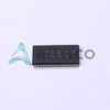
SN74CBTD16210DGGR (1)
Manufacturer Part Number
SN74CBTD16210DGGR
Manufacturer
Texas Instruments
Introduction
High-bandwidth bus switch designed for routing signals with minimal propagation delay.
Product Features and Performance
High-speed signal switching
Low crosstalk
Low bit-to-bit skew
Quick turn-on and turn-off times
5-ohm switch connection between two ports
Minimal power consumption
Product Advantages
Reduces signal distortion
Enhances system performance in high-speed applications
Provides improved signal integrity
Ease of signal routing in complex circuits
Robust design for high reliability

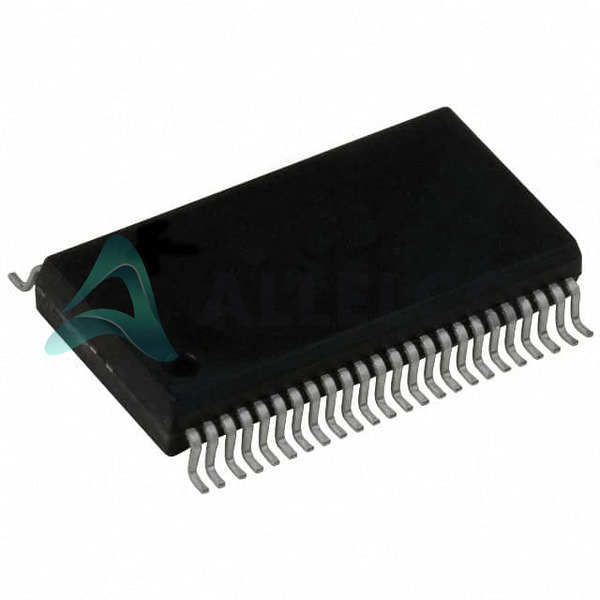
SN74CBTD16210DGGR (2)
Key Technical Parameters
10 x 1:1 bus switch configuration
Two independent circuits
Single supply voltage: 4.5V ~ 5.5V
Available in 48-TFSOP package
Operating Temperature range: -40°C to 85°C
Quality and Safety Features
Built-in over-voltage tolerance
Robust ESD protection
Compatibility
Compatible with TTL (Transistor-Transistor Logic) levels
Interoperable with a wide range of digital ICs
Application Areas
High-speed data transmission paths
Communication systems
Servers and networking equipment
Computer peripherals
Signal routing applications
Product Lifecycle
Status: Active
Continued manufacturing with no near-term discontinuation
Replacements or upgrades: Please consult Texas Instruments for future products
Several Key Reasons to Choose This Product
High signal bandwidth conserves signal integrity in fast systems
Reduced latency enhances overall system performance
Flexibility in handling multiple data paths
Durable construction for long-term reliability
Supported by Texas Instruments' commitment to quality and long-term availability


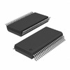 SN74CBTD16210DLTexas InstrumentsIC BUS SWITCH 10 X 1:1 48SSOP
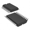 SN74CBT6845CDWTexas InstrumentsIC BUS SWITCH 8 X 1:1 20SOIC
 SN74CBT6845CPWTexas InstrumentsIC BUS SWITCH 8 X 1:1 20TSSOP
 SN74CBT6845CDGVRTexas InstrumentsIC BUS SWITCH 8 X 1:1 20TVSOP
 SN74CBT6845CRGYRTexas InstrumentsIC BUS SWITCH 8 X 1:1 20VQFN


