View All

Please refer to the English Version as our Official Version.Return

Europe
France(Français) Germany(Deutsch) Italy(Italia) Russian(русский) Poland(polski) Czech(Čeština) Luxembourg(Lëtzebuergesch) Netherlands(Nederland) Iceland(íslenska) Hungarian(Magyarország) Spain(español) Portugal(Português) Turkey(Türk dili) Bulgaria(Български език) Ukraine(Україна) Greece(Ελλάδα) Israel(עִבְרִית) Sweden(Svenska) Finland(Svenska) Finland(Suomi) Romania(românesc) Moldova(românesc) Slovakia(Slovenská) Denmark(Dansk) Slovenia(Slovenija) Slovenia(Hrvatska) Croatia(Hrvatska) Serbia(Hrvatska) Montenegro(Hrvatska) Bosnia and Herzegovina(Hrvatska) Lithuania(lietuvių) Spain(Português) Switzerland(Deutsch) United Kingdom(English)
Asia/Pacific
Japan(日本語) Korea(한국의) Thailand(ภาษาไทย) Malaysia(Melayu) Singapore(Melayu) Vietnam(Tiếng Việt) Philippines(Pilipino)
Africa, India and Middle East
United Arab Emirates(العربية) Iran(فارسی) Tajikistan(فارسی) India(हिंदी) Madagascar(malaɡasʲ)
South America / Oceania
New Zealand(Maori) Brazil(Português) Angola(Português) Mozambique(Português)
North America
United States(English) Canada(English) Haiti(Ayiti) Mexico(español)
HomeProductsIntegrated Circuits (ICs)PMIC - Voltage Regulators - DC DC Switching RegulatorsTPS62693YFDT
TPS62693YFDT Image
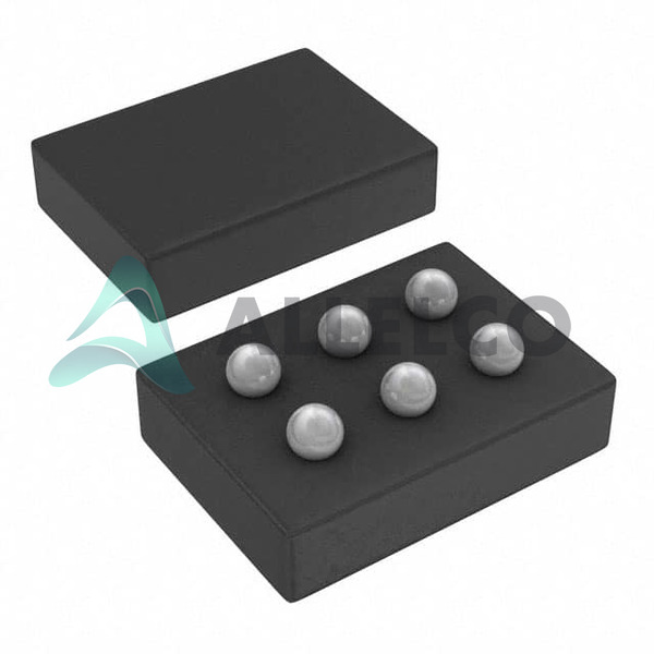
Image may be representation.
See specifications for product details.
EXPRESS OPTION
Payment method

TPS62693YFDT - Texas Instruments

Manufacturer Part Number
TPS62693YFDT
Manufacturer
Texas Instruments
Allelco Part Number
98D-TPS62693YFDT
Warranty
1 Year Allelco Warranty - Find out more
Stock Status:
49,274 pcs available, New & Original
Parts Description
IC REG BUCK 2.85V 800MA 6DSBGA
Package
6-DSBGA
Data sheet
TPS62693YFDT.pdf
RoHs Status
ROHS3 Compliant
Our certification
In stock: 49274
  • Unit Price: $0.836
  • Subtotal: $0.00

Want a better price?
Add to Cart and Submit RFQ now, we'll contact you immediately.

Quantity Unit Price Ext. Price
1+ $0.836 $0.84
The above prices does not include taxes and freight rates, which will be calculated on the order pages.

Specifications

TPS62693YFDT Tech Specifications
Texas Instruments - TPS62693YFDT technical specifications, attributes, parameters and parts with similar specifications to Texas Instruments - TPS62693YFDT

Product Attribute Attribute Value
Manufacturer Texas Instruments
Voltage - Output (Min/Fixed) 2.85V
Voltage - Output (Max) -
Voltage - Input (Min) 2.3V
Voltage - Input (Max) 4.8V
Topology Buck
Synchronous Rectifier Yes
Supplier Device Package 6-DSBGA
Series -
Package / Case 6-XFBGA, DSBGA
Product Attribute Attribute Value
Package Tape & Reel (TR)
Output Type Fixed
Output Configuration Positive
Operating Temperature -40°C ~ 85°C (TA)
Number of Outputs 1
Mounting Type Surface Mount
Function Step-Down
Frequency - Switching 3MHz
Current - Output 800mA
Base Product Number TPS62693

Environmental & Export Classifications

ATTRIBUTE DESCRIPTION
RoHs Status ROHS3 Compliant
Moisture Sensitivity Level (MSL) 1 (Unlimited)
REACH Status REACH Unaffected
ECCN EAR99
HTSUS 8542.39.0001

Frequently Asked Questions(FAQ)

What are the key electrical characteristics of the TPS62693YFDT buck regulator that make it suitable for space-constrained, high-efficiency power applications?
The TPS62693YFDT delivers a fixed 2.85V output at up to 800mA with a switching frequency of 3MHz, enabling smaller external components such as inductors and capacitors due to higher operating frequency. Its input voltage range spans from 2.3V to 4.8V, supporting a broad spectrum of battery-powered systems. With synchronous rectification, it achieves high efficiency—typically above 90% under moderate load conditions—minimizing heat dissipation in compact designs. The 6-DSBGA package occupies minimal board area while maintaining reliable performance across an industrial temperature range of -40°C to 85°C.
How does the TPS62693YFDT compare to other members of the TPS62693 family in terms of output current and thermal management?
While the TPS62693YFDT is rated for 800mA output current, other variants in the TPS62693 series may support lower or higher current limits depending on package and thermal constraints. For instance, some versions may be optimized for 500mA or 1A, trading off component count or footprint for specific application needs. The YF variant’s DSBGA packaging provides excellent thermal conductivity but limits current handling compared to larger packages like WSON, which can dissipate more heat. Designers must evaluate both output requirements and ambient operating conditions when selecting among these options.
Can the TPS62693YFDT operate reliably from a single Li-ion cell without additional voltage boosting?
Yes, the TPS62693YFDT can directly regulate a single Li-ion cell, which typically discharges from about 4.2V down to 2.7V. Since the device supports an input range of 2.3V to 4.8V, it maintains stable 2.85V regulation even as the battery voltage drops near its end-of-life threshold. This eliminates the need for a boost converter at light loads, simplifying system architecture and improving efficiency during deep discharge phases.
What considerations apply when integrating the TPS62693YFDT into a layout with strict electromagnetic compatibility (EMC) requirements?
Due to its 3MHz switching frequency, the TPS62693YFDT emits energy in a band that can interfere with nearby RF circuits or sensitive analog signals if not properly managed. A well-designed PCB layout—featuring short traces for high-current paths, adequate ground planes, and low-ESR ceramic input/output capacitors placed close to the IC—is essential. Additionally, using shielded inductors and minimizing loop area reduces radiated emissions. Careful filtering and shielding may still be required in Class B EMC environments.
Is it feasible to use the TPS62693YFDT in a multi-output power supply configuration requiring one rail at 2.85V and another at 1.8V?
No, the TPS62693YFDT provides only a single fixed 2.85V output. To generate multiple voltage rails such as 2.85V and 1.8V, an additional regulator—either another TPS62693YFDT tuned via feedback resistors (if adjustable) or a different topology like LDO or buck converter—would be required. Alternatively, a dual-output switching regulator or post-regulation using linear stages could be considered, but each introduces complexity, cost, and potential efficiency trade-offs.
How does the TPS62693YFDT handle transient load steps, and what external components influence its response time?
The TPS62693YFDT features internal compensation designed for stable operation across typical load steps. However, the speed and magnitude of transient response depend significantly on the output capacitor selection, particularly the equivalent series resistance (ESR). Low-ESR ceramic capacitors improve transient recovery by providing rapid charge injection during sudden current demands. The inductor value also plays a role: lower inductance allows faster current slew rates but increases ripple. Proper tuning of C_out and L ensures minimal output deviation during load transients without excessive overshoot.
What are the implications of using the TPS62693YFDT near its maximum output current rating under continuous operation?
Operating the TPS62693YFDT near 800mA continuously increases internal power dissipation, especially when the input-to-output differential voltage is large. For example, at V_in = 4.8V and I_out = 800mA, power loss can exceed 1W if conduction and switching losses accumulate significantly. This raises junction temperature, potentially exceeding safe limits without adequate PCB copper area or airflow. Thermal derating curves should be consulted to ensure reliability; otherwise, reduced current capability or added heatsinking may be necessary.
Why might a designer choose the TPS62693YFDT over an LDO for a 2.85V supply derived from a 3.7V battery?
Although LDOs are simple and quiet, they waste excess voltage as heat. If the battery averages around 3.7V, a traditional LDO delivering 2.85V would dissipate roughly (3.7–2.85) × 0.8 ≈ 0.72W at full load, requiring significant thermal management. In contrast, the TPS62693YFDT uses switching topology to minimize this loss, achieving efficiencies upwards of 85–90%. This makes it far more suitable for long battery life, compact form factors, and thermally constrained environments where LDO solutions would overheat.
How does the Moisture Sensitivity Level (MSL) of 1 for the TPS62693YFDT affect handling in automated assembly processes?
An MSL rating of 1 indicates unlimited floor life under normal storage conditions, meaning the TPS62693YFDT can be handled without special precautions before reflow soldering. This simplifies inventory management and assembly workflows, particularly in high-volume production lines. It also reduces the risk of moisture-induced defects during reflow, eliminating the need for baking prior to use in most manufacturing scenarios.
Can the TPS62693YFDT be used in automotive-grade applications given its industrial temperature range?
The TPS62693YFDT is specified for operation from -40°C to 85°C, which aligns with many automotive infotainment and body electronics subsystems but falls short of full AEC-Q100 qualification for mission-critical power stages. While acceptable for non-safety-related modules, designers targeting full automotive compliance should verify qualification status or consider alternative parts with explicit AEC-Q100 Grade 1 (-40°C to +125°C) certification. Environmental stress screening and reliability testing beyond datasheet guarantees may still be advisable depending on application criticality.
What role does the base product number TPS62693 play in selecting compatible evaluation boards or reference designs?
The base model TPS62693 encompasses several package and pinout variations, including the YF (DSBGA) variant used in the TPS62693YFDT. When sourcing evaluation modules or schematic references, specifying the complete part number ensures correct pin mapping and thermal characteristics. Some reference designs may list only the base number, so verifying compatibility between the evaluation kit and target footprint is essential to avoid layout errors or functional mismatches during prototyping.
How do RoHS 3 and REACH compliance of the TPS62693YFDT impact material sourcing and regulatory reporting in global markets?
RoHS 3 compliance confirms absence of restricted substances such as lead, mercury, and cadmium, meeting EU and international environmental regulations. REACH unaffected status indicates no registration obligations for SVHCs (Substances of Very High Concern), reducing administrative overhead in supply chain documentation. These designations simplify export procedures and enhance trust with OEMs requiring conflict-free and environmentally responsible sourcing, particularly in consumer electronics and medical devices.
What precautions should be taken when replacing the TPS62693YFDT with a functionally similar regulator in legacy designs?
Direct substitution requires matching not just voltage and current specs but also switching frequency, feedback structure, and pinout geometry. The 6-DSBGA package has fine-pitch bonds that demand precise pick-and-place alignment; mismatched footprints risk shorting adjacent pads or poor solder joint formation. Additionally, control-loop dynamics differ between regulators—even with similar topologies—so stability margins, startup behavior, and EMI profiles may vary. Prototyping and bench testing are strongly recommended before committing to a replacement.
How does the 3MHz switching frequency of the TPS62693YFDT influence component selection compared to lower-frequency alternatives?
The 3MHz frequency allows use of smaller magnetics and capacitors due to relaxed requirements on inductance and capacitance values. For instance, a 0.47µH inductor suffices instead of a 2.2µH part seen at 500kHz, reducing board space and cost. However, higher-frequency operation increases core losses in inductors and ESR-related switching losses in capacitors, potentially lowering peak efficiency slightly. Noise spectra shift upward, demanding better filtering in mixed-signal systems. Overall, it favors miniaturization over marginal efficiency gains.
Can the TPS62693YFDT enter a low-power shutdown mode to reduce quiescent current?
Yes, the TPS62693YFDT supports a shutdown feature where input current drops to microamps, effectively disabling the regulator. This enables ultra-low standby power consumption in battery-operated devices. During shutdown, the output floats, so external circuitry must prevent backfeeding from downstream loads. Activation is typically controlled via an enable pin tied to a microcontroller or power management IC, allowing dynamic power gating based on system state.
What are the risks of operating the TPS62693YFDT outside its recommended input voltage range?
Exceeding the 4.8V maximum input voltage can damage internal gate drivers or cause latch-up in CMOS structures, leading to permanent failure. Similarly, dropping below 2.3V may prevent proper regulation or force dropout, causing output instability. Even brief excursions beyond these bounds—such as from inductive kickback or improper hot-plug sequencing—can compromise reliability. Input protection diodes or TVS devices may be added to clamp transients, but sustained out-of-range operation violates absolute maximum ratings and voids warranty.

Parts with Similar Specifications

The three parts on the right have similar specifications to Texas Instruments TPS62693YFDT

Product Attribute TPS62693YFDR TPS62697YFFT TPS62692YFDR TPS62690YFFT
Part Number TPS62693YFDR TPS62697YFFT TPS62692YFDR TPS62690YFFT
Manufacturer Texas Instruments Texas Instruments Texas Instruments Texas Instruments
Series - - - -
Supplier Device Package - 196-NFBGA (12x12) 16-PDIP 64-VQFN (9x9)
Mounting Type - Surface Mount Through Hole Surface Mount
Topology - - - -
Package / Case - 196-LFBGA 16-DIP (0.300', 7.62mm) 64-VFQFN Exposed Pad
Voltage - Output (Min/Fixed) - - - -
Base Product Number - DAC34H84 MAX500 ADS62P42
Frequency - Switching - - - -
Function - - - -
Voltage - Output (Max) - - - -
Synchronous Rectifier - - - -
Voltage - Input (Min) - - - -
Operating Temperature - -40°C ~ 85°C 0°C ~ 70°C -40°C ~ 85°C
Package - Tape & Reel (TR) Tube Tape & Reel (TR)
Number of Outputs - - - -
Current - Output - - - -
Voltage - Input (Max) - - - -
Output Type - Current - Unbuffered Voltage - Buffered -
Output Configuration - - - -

TPS62693YFDT Datasheet PDF

Download TPS62693YFDT pdf datasheets and Texas Instruments documentation for TPS62693YFDT - Texas Instruments.

PCN Design/Specification
DSBGA/uSIP 22/Jun/2016.pdf DSBGA/Usip 14/Sep/2016.pdf
PCN Packaging
Carrier Tape 28/Aug/2018.pdf WCSP Pin Indicator 15/Jan/2021.pdf
HTML Datasheet
TPS6269x.pdf

Customer Reviews

Evaluation: 10 Articles

  • Nath***rooks
    Jun 11, 2026

    Installed this power component in a converter board. Output remained stable under different load conditions and thermal performance was better than expected.

  • Dani***alkerTech
    Jun 1, 2026

    Product works, but setup took more effort than expected. Once configured the MCU ran reliably, although documentation support felt older compared with newer platforms. Fine for maintenance projects.

  • Yuki***aka88
    May 26, 2026

    信号通信プロジェクトでこのRS-485トランシーバーを使用しました。設置は簡単で、長距離ケーブルでも通信は安定していました。消費電力も、以前使用していたものより低くなっています。

  • Stev***aker
    May 20, 2026

    Solid diode for power rectification. Works well in switching circuits.

  • Bran***Lewis
    May 11, 2026

    Compact FPGA with good performance. Suitable for basic signal processing tasks.

  • Oliv***arris
    May 7, 2026

    Reliable I/O expander. Works well in embedded control applications.

  • Jess***Jones
    Apr 17, 2026

    It offers good value for the price, and the specifications match the description. I’ve been using it for two days with no issues, and I’ll definitely buy it again if I need it in the future.

  • Mich***Smith
    Apr 17, 2026

    Shipping was on time, the component pins are neatly aligned, and I tested 10 of them with a multimeter—all readings were within the specified range. Highly recommended.

  • Aman***arris
    Apr 3, 2026

    It was great—the entire process, from placing the order to receiving the package, went very smoothly. The components were consistent, the price was fair, and I had a very pleasant shopping experience.

  • Mike***nch
    Apr 3, 2026

    Better than expected! The resistance and capacitance readings were spot-on, and it passed the test on the first try. The service was reliable, and the packaging was thoughtful—I highly recommend it.

Write a Review

Your Email address will not be published.

Shipment

Delivery Time

In-stock items can be shipped within 24 hours. Some parts will be arranged for delivery within 1-2 days from the date all items arrive at our warehouse. And Allelco ships order once a day at about 17:00, except Sunday. Once the goods are shipped, the estimated delivery time depends on the shipping methods and Delivery destination. The table below shows are the logistic time for some common countries.

Delivery Cost

  1. Use your express account for shipment if you have one.
  2. Use our account for the shipment. Refer to the table below for the approximate charges.
(Different time frame / countries / package size has different price.)

Delivery Method

  1. Global Common Shipment by DHL / UPS / FedEx / TNT / EMS / SF we support.
  2. Others more shipping ways, please get in touch with your customer manager.

Common Countries Logistic Time Reference
Region Country Logistic Time(Day)
America United States 5
Brazil 7
Europe Germany 5
United Kingdom 4
Italy 5
Oceania Australia 6
New Zealand 5
Asia India 4
Japan 4
Middle East Israel 6
DHL & FedEx Shipment Charges Reference
Shipment charges(KG) Reference DHL(USD$)
0.00kg-1.00kg USD$30.00 - USD$60.00
1.00kg-2.00kg USD$40.00 - USD$80.00
2.00kg-3.00kg USD$50.00 - USD$100.00
Note:
The above table is for reference only. There may have some data bias for the uncontrollable factors.
Contact us if you have any questions.
  • QC (Quality Warranty)
  • Payment Support
  • Packaging
  • Certifications & Memberships

QC (Quality Warranty)

Allelco is committed to exceeding customer expectations through customer service excellence, order accuracy, and on-time delivery.
This is achieved through our commitment to the continual improvement of our processes, services, and products.


Strict quality inspection builds a solid foundation for electronic component quality.
  1. Visual inspection
  2. Performance testing and reliability verification
  3. Standardized full-process testing
  4. Precise control of every parameter
We eliminate defective components and ensure the stable operation of electronic devices through professional quality standards.

Payment Support

The payment method can be chosen from the methods shown below: Wire Transfer (T/T, Bank Transfer), Western Union, Credit card, PayPal.
  • HKBea
  • Paypal
  • MasterCard
  • Western-Union
  • VISA
Stable Delivery, Sincere Partnership — Your Faithful Supply Chain Partner
  • Efficient Supply Management
  • Cost-Saving Procurement
  • Fast Sourcing & Delivery
Contact us if you have any questions.

Packaging

Electrostatic Discharge Protection and Handling

All electrostatic-sensitive components are handled in accordance with electrostatic discharge control procedures. The products are hermetically sealed in anti-static safe packaging to prevent electrostatic damage. Appropriate labeling is also applied for identification and traceability. This ensures product integrity during storage, handling and transportation.


ESD

Certifications & Memberships

Third-party certified, strict quality control. Our certification
  • ISO 9001: 2015
  • ISO 13485: 2016
  • ISO 14001: 2015
  • ISO 28000: 2007
  • ISO 45001: 2018
  • GB/T 27922-2011
  • SMTA
  • IPC
  • ESD
  • PSMA
TPS62693YFDT Image

TPS62693YFDT

Texas Instruments
98D-TPS62693YFDT

Want a better price? Add to Cart and Submit RFQ now, we'll contact you immediately.

0 RFQ
Shopping cart (0 Items)
It is empty.
Compare List (0 Items)
It is empty.
Feedback

Your feedback matters! At Allelco, we value the user experience and strive to improve it constantly.
Please share your comments with us via our feedback form, and we'll respond promptly.
Thank you for choosing Allelco.

Subject
E-mail
Comments
Captcha
Drag or click to upload file
Upload File
types: .xls, .xlsx, .doc, .docx, .jpg, .png and .pdf.
Max file size: 10MB